JAJSRK1G March 2012 – November 2023 TPS7A7100
PRODUCTION DATA
- 1
- 1 特長
- 2 アプリケーション
- 3 概要
- 4 Pin Configurations
- 5 Specifications
- 6 Detailed Description
- 7 Application and Implementation
- 8 Device And Documentation Support
- 9 Revision History
- 10Mechanical, Packaging, And Orderable Information
パッケージ・オプション
メカニカル・データ(パッケージ|ピン)
サーマルパッド・メカニカル・データ
- RGT|16
発注情報
4 Pin Configurations
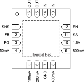
 Figure 4-1 RGT Package,16-Pin VQFN(Top View)
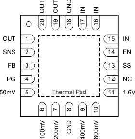
 Figure 4-2 RGW Package,20-Pin VQFN With Exposed Thermal Pad(Top View)
Table 4-1 Pin Functions
| PIN | I/O | DESCRIPTION | ||
|---|---|---|---|---|
| NAME | RGW | RGT | ||
| 50mV, 100mV, 200mV, 400mV, 800mV, 1.6V | 5, 6, 7, 9, 10, 11 |
4, 5, 6, 8, 9, 10 |
I | Output voltage setting pins. These pins must be connected to ground or left floating. Connecting these pins to ground increases the output voltage by the value of the pin name; multiple pins can be simultaneously connected to GND to select the desired output voltage. Leave these pins floating (open) when not in use. See the User-Configurable Output Voltage section for more details. |
| EN | 14 | 12 | I | Enable pin. Driving this pin to logic high enables the device; driving the pin to logic low disables the device. See the Enable section for more details. |
| FB | 3 | 2 | I | Output voltage feedback pin. Connected to the error amplifier. See the User-Configurable Output Voltage and Traditional Adjustable Configuration sections for more details. Connect a 220-pF ceramic capacitor from the FB pin to OUT. |
| GND | 8, 18 | 7 | — | Ground pin. |
| IN | 15, 16, 17 | 13, 14 | I | Unregulated supply voltage pin. Connect an input capacitor to this pin. See the Input Capacitor Requirements section for more details. |
| NC | 12 | — | — | Not internally connected. The NC pin is not connected to any electrical node. This pin and the thermal pad must be connected to a large-area ground plane. See the Power Dissipation section for more details. |
| OUT | 1, 19, 20 | 15, 16 | O | Regulated output pin. A 4.7-μF or larger capacitance is required for stability. See the Output Capacitor Requirements section for more details. |
| PG | 4 | 3 | O | Active-high power good pin. An open-drain output that indicates when the output voltage reaches 90% of the target. See the Power-Good section for more details. |
| SNS | 2 | 1 | I | Output voltage sense input pin. See the User-Configurable Output Voltage and Traditional Adjustable Configuration sections for more details. |
| SS | 13 | 11 | — | Soft-start pin. Leaving this pin open provides a soft start of the
default setting. Connecting an external capacitor between this pin and ground enables the soft-start function by forming an RC-delay circuit in combination with the integrated resistance on the silicon. See the Soft-Start section for more details. |
| Thermal Pad | — | The thermal pad must be connected to a large-area ground plane. If available, connect an electrically-floating, dedicated thermal plane to the thermal pad as well. | ||