JAJSCT1 December 2016 TPS7A91
PRODUCTION DATA.
- 1 特長
- 2 アプリケーション
- 3 概要
- 4 改訂履歴
- 5 Pin Configuration and Functions
- 6 Specifications
-
7 Detailed Description
- 7.1 Overview
- 7.2 Functional Block Diagram
- 7.3 Feature Description
- 7.4 Device Functional Modes
- 8 Application and Implementation
- 9 Power Supply Recommendations
- 10Layout
- 11デバイスおよびドキュメントのサポート
- 12メカニカル、パッケージ、および注文情報
10 Layout
10.1 Layout Guidelines
General guidelines for linear regulator designs are to place all circuit components on the same side of the circuit board and as near as practical to the respective LDO pin connections. Place ground return connections to the input and output capacitors, and to the LDO ground pin as close to each other as possible, connected by a wide, component-side, copper surface. The use of vias and long traces to create LDO circuit connections is strongly discouraged and negatively affects system performance.
10.1.1 Board Layout
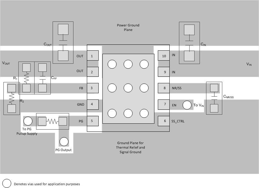
To maximize the ac performance of the TPS7A91, following the layout example illustrated in Figure 42 is recommended. This layout isolates the analog ground (AGND) from the noisy power ground. Components that must be connected to the quiet analog ground are the noise reduction capacitor (CNR/SS) and the lower feedback resistor (R2). These components must have a separate connection back to the power pad of the device for optimal output noise performance. Connect the GND pin directly to the thermal pad and not to any external plane.
To maximize the output voltage accuracy, the connection from the output voltage back to top output divider resistors (R1) must be made as close as possible to the load. This method of connecting the feedback trace eliminates the voltage drop from the device output to the load.
To improve thermal performance, use an array of thermal vias to connect the thermal pad to the ground planes. Larger ground planes improve the thermal performance of the device and lowering the operating temperature of the device.
10.2 Layout Example
 Figure 42. TPS7A91 Example Layout