JAJSMN7C september 2021 – june 2023 TPS7A94
PRODUCTION DATA
- 1
- 1 特長
- 2 アプリケーション
- 3 概要
- 4 Revision History
- 5 Pin Configuration and Functions
- 6 Specifications
-
7 Detailed Description
- 7.1 Overview
- 7.2 Functional Block Diagram
- 7.3
Feature Description
- 7.3.1 Output Voltage Setting and Regulation
- 7.3.2 Ultra-Low Noise and Ultra-High Power-Supply Rejection Ratio (PSRR)
- 7.3.3 Programmable Current Limit and Power-Good Threshold
- 7.3.4 Programmable Soft Start (NR/SS Pin)
- 7.3.5 Precision Enable and UVLO
- 7.3.6 Active Discharge
- 7.3.7 Thermal Shutdown Protection (TSD)
- 7.4 Device Functional Modes
-
8 Application and Implementation
- 8.1
Application Information
- 8.1.1 Output Voltage Restart (Overshoot Prevention Circuit)
- 8.1.2 Precision Enable (External UVLO)
- 8.1.3 Undervoltage Lockout (UVLO) Operation
- 8.1.4 Dropout Voltage (VDO)
- 8.1.5 Power-Good Feedback (FB_PG Pin) and Power-Good Threshold (PG Pin)
- 8.1.6 Adjusting the Factory-Programmed Current Limit
- 8.1.7 Programmable Soft-Start and Noise-Reduction (NR/SS Pin)
- 8.1.8 Inrush Current
- 8.1.9 Optimizing Noise and PSRR
- 8.1.10 Adjustable Operation
- 8.1.11 Paralleling for Higher Output Current and Lower Noise
- 8.1.12 Recommended Capacitor Types
- 8.1.13 Load Transient Response
- 8.1.14 Power Dissipation (PD)
- 8.1.15 Estimating Junction Temperature
- 8.1.16 TPS7A94EVM-046 Thermal Analysis
- 8.2 Typical Application
- 8.3 Power Supply Recommendations
- 8.4 Layout
- 8.1
Application Information
- 9 Device and Documentation Support
- 10Mechanical, Packaging, and Orderable Information
パッケージ・オプション
デバイスごとのパッケージ図は、PDF版データシートをご参照ください。
メカニカル・データ(パッケージ|ピン)
- DSC|10
サーマルパッド・メカニカル・データ
発注情報
8.1.3 Undervoltage Lockout (UVLO) Operation
The UVLO circuit, present on the IN pin, ensures that the device remains disabled before the input supply reaches the minimum operational voltage range, and that the device shuts down when the input supply falls too low.
The UVLOIN circuit has a minimum response time of several microseconds to fully assert. During this time, a downward line transient below approximately 1.6 V causes the input supply UVLO to assert for a short time. However, the UVLOIN circuit can possibly not have enough stored energy to fully discharge the internal circuits inside of the device. When the UVLOIN circuit does not fully discharge, internal circuitry is not fully disabled.
The effect of the downward line transient can trigger the overshoot prevention circuit and can be easily mitigated by using the solution proposed in the Precision Enable (External UVLO)Precision Enable (External UVLO)Precision Enable (External UVLO) section.
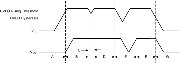
Figure 8-7 illustrates the UVLOIN circuit response to various input voltage events. This diagram can be separated into the following regions:
- Region A: The device does not turn on until the input reaches the UVLO rising threshold.
- Region B: Normal operation with a regulated output.
- Region C: Brownout event above the UVLO falling threshold (UVLO rising threshold – UVLO hysteresis). The output can fall out of regulation but the device is still enabled.
- Region D: Normal operation with a regulated output.
- Region E: Brownout event below the UVLO falling threshold. The device is disabled in most cases and the output falls because of the load and active discharge circuit. The device is re-enabled when the UVLO rising threshold is reached by the input voltage and a normal start up then follows.
- Region F: Normal operation followed by the input falling to the UVLO falling threshold.
- Region G: The device is disabled when the input voltage falls below the UVLO falling threshold to 0 V. The output falls because of the load and active discharge circuit.
 Figure 8-7 Typical
UVLO Operation