JAJSM29A april 2023 – july 2023 TPS7A96
PRODUCTION DATA
- 1
- 1 特長
- 2 アプリケーション
- 3 概要
- 4 Revision History
- 5 Pin Configuration and Functions
- 6 Specifications
-
7 Detailed Description
- 7.1 Overview
- 7.2 Functional Block Diagram
- 7.3
Feature Description
- 7.3.1 Output Voltage Setting and Regulation
- 7.3.2 Ultra-Low Noise and Ultra-High Power-Supply Rejection Ratio (PSRR)
- 7.3.3 Programmable Current Limit and Power-Good Threshold
- 7.3.4 Programmable Soft-Start (NR/SS Pin)
- 7.3.5 Precision Enable and UVLOs
- 7.3.6 Active Discharge
- 7.3.7 Thermal Shutdown Protection (TSD)
- 7.4 Device Functional Modes
-
8 Application and Implementation
- 8.1
Application Information
- 8.1.1 Output Voltage Restart (Overshoot Prevention Circuit)
- 8.1.2 Precision Enable (External UVLO)
- 8.1.3 Undervoltage Lockout (UVLO) Operation
- 8.1.4 Dropout Voltage (VDO)
- 8.1.5 Power-Good Feedback (FB_PG Pin) and Power-Good Threshold (PG Pin)
- 8.1.6 Adjusting the Factory-Programmed Current Limit
- 8.1.7 Programmable Soft-Start and Noise-Reduction (NR/SS Pin)
- 8.1.8 Inrush Current
- 8.1.9 Optimizing Noise and PSRR
- 8.1.10 Adjustable Operation
- 8.1.11 Paralleling for Higher Output Current and Lower Noise
- 8.1.12 Recommended Capacitor Types
- 8.1.13 Load Transient Response
- 8.1.14 Power Dissipation (PD)
- 8.1.15 Estimating Junction Temperature
- 8.1.16 TPS7A96EVM-106 Thermal Analysis
- 8.2 Typical Application
- 8.3 Power Supply Recommendations
- 8.4 Layout
- 8.1
Application Information
- 9 Device and Documentation Support
- 10Mechanical, Packaging, and Orderable Information
パッケージ・オプション
メカニカル・データ(パッケージ|ピン)
- DSC|10
サーマルパッド・メカニカル・データ
- DSC|10
発注情報
8.1.1 Output Voltage Restart (Overshoot Prevention Circuit)
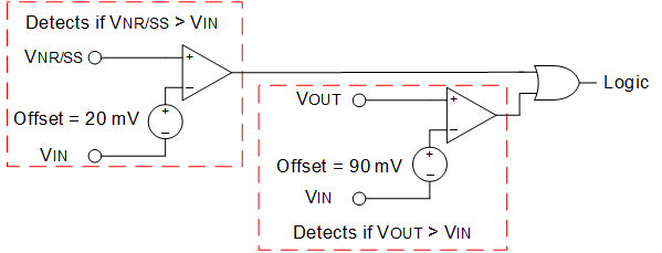
Wide bandwidth linear regulators suffer from an undesirable excessive overshooting of the output voltage during restart events that occur when the CNR/SS and COUT capacitors are not fully discharged. In this device, and as shown in Figure 8-1, this undesirable behavior is mitigated by implementing low hysteresis circuitry consisting of two ORed comparators to detect when the input voltage is either 20 mV (typical) lower than the VNR/SS reference voltage or 300 mV (typical) lower than VOUT.
 Figure 8-1 Overshoot Prevention
Circuit
Figure 8-1 Overshoot Prevention
CircuitWhen the device is operating in dropout, transient events (such as an input voltage brownout, heavy load transient, or short-circuit event) can force the device in a reversed bias condition where the input voltage is either 20 mV (typical) lower than the VNR/SS reference voltage or 300 mV (typical) lower than VOUT. The output overshoot prevention circuit can be triggered, as shown in Figure 8-2, thus forcing the device to shutdown and restart, thereby preventing output voltage overshoot. If the device is still operating in dropout and the error condition that triggered this circuit is still present, an additional restart can occur until these conditions are removed or the device is no longer in dropout. The restart always occurs from a discharged state and always has the same characteristics as the initial LDO power-up, so the start-up time, VOUT ramp rate, and VOUT monotonicity are all predictable.
 Figure 8-2 Device Behavior in
Dropout
Figure 8-2 Device Behavior in
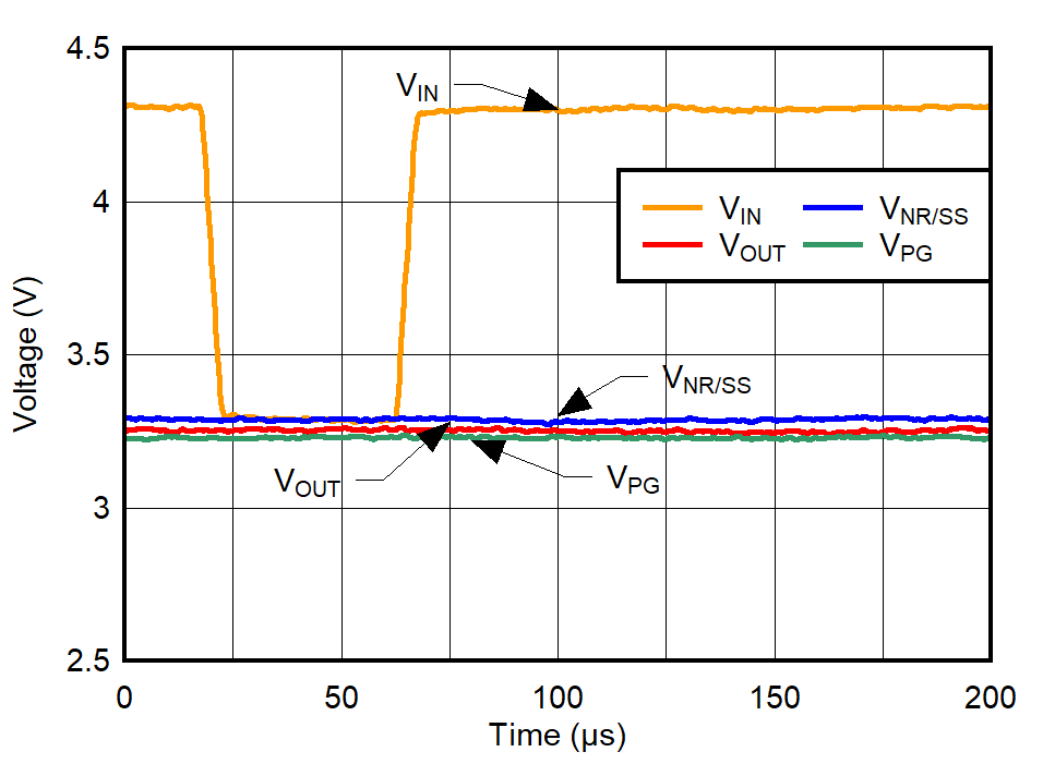
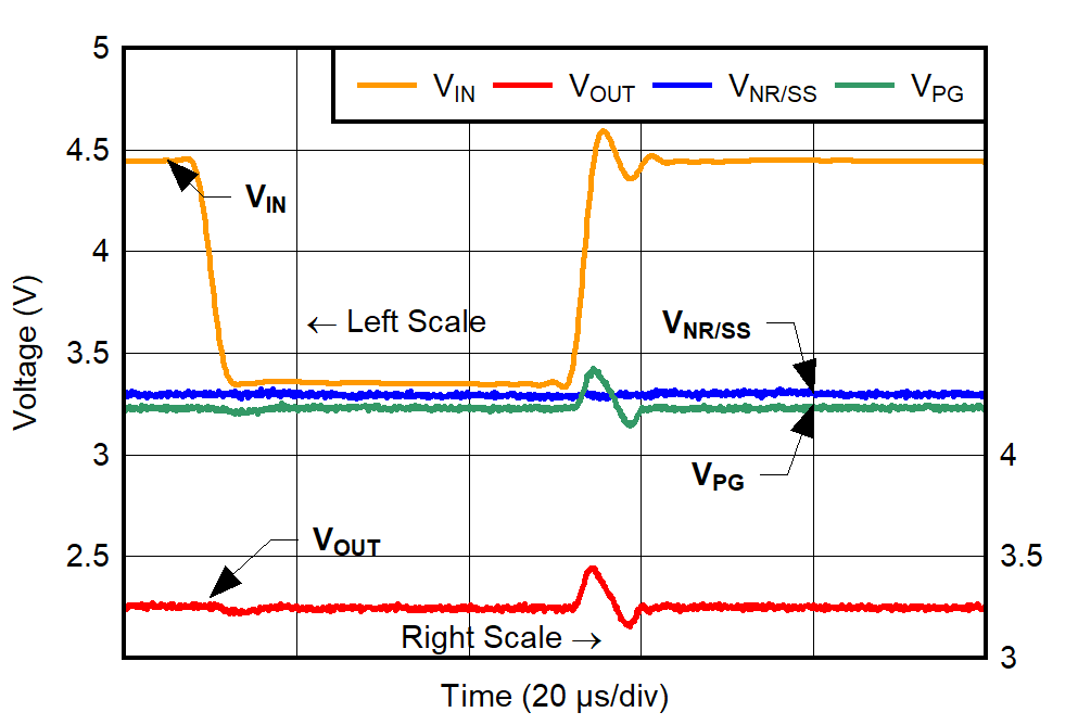
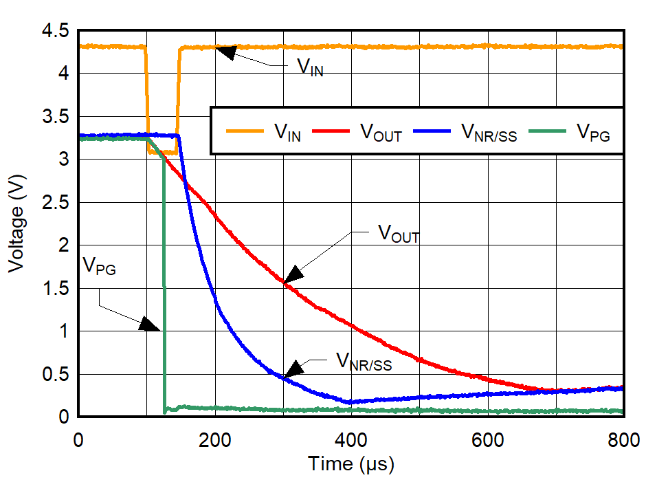
DropoutFigure 8-3 and Figure 8-4 show examples of a soft brownout and a brownout event, respectively.
The brownout overshoot is present with higher VIN slew rates. A 1-V/μs slew rate was used in Figure 8-5.
 Figure 8-3 Example: Soft Brownout to
VNR/SS
 Figure 8-5 Example: Brownout With
Overshoot Recovery
 Figure 8-4 Example: Brownout
The overshoot prevention circuit is implemented to provide a predictable start-up and shutdown of the device without output overshoot if the EN_UV external UVLO is not used as described in this section. This circuit can be prevented from triggering by:
- Using an input supply capable of handling heavy load transients or a larger value input capacitor
- Increasing the operating headroom between VIN and VOUT (for example, when using a battery as an input supply to make sure that VIN stays higher than VOUT even when the battery is near the full discharge state)
- Using an input supply with a ramp rate faster than the set output voltage time constant formed by CNR/SS || RNR/SS
- Discharging the input supply slower than the discharge time formed by COUT || (Load || RPULLDOWN) or by the CNR/SS || (RNR/SS || RPULLDOWN_NR/SS)