JAJSM29A april 2023 – july 2023 TPS7A96
PRODUCTION DATA
- 1
- 1 特長
- 2 アプリケーション
- 3 概要
- 4 Revision History
- 5 Pin Configuration and Functions
- 6 Specifications
-
7 Detailed Description
- 7.1 Overview
- 7.2 Functional Block Diagram
- 7.3
Feature Description
- 7.3.1 Output Voltage Setting and Regulation
- 7.3.2 Ultra-Low Noise and Ultra-High Power-Supply Rejection Ratio (PSRR)
- 7.3.3 Programmable Current Limit and Power-Good Threshold
- 7.3.4 Programmable Soft-Start (NR/SS Pin)
- 7.3.5 Precision Enable and UVLOs
- 7.3.6 Active Discharge
- 7.3.7 Thermal Shutdown Protection (TSD)
- 7.4 Device Functional Modes
-
8 Application and Implementation
- 8.1
Application Information
- 8.1.1 Output Voltage Restart (Overshoot Prevention Circuit)
- 8.1.2 Precision Enable (External UVLO)
- 8.1.3 Undervoltage Lockout (UVLO) Operation
- 8.1.4 Dropout Voltage (VDO)
- 8.1.5 Power-Good Feedback (FB_PG Pin) and Power-Good Threshold (PG Pin)
- 8.1.6 Adjusting the Factory-Programmed Current Limit
- 8.1.7 Programmable Soft-Start and Noise-Reduction (NR/SS Pin)
- 8.1.8 Inrush Current
- 8.1.9 Optimizing Noise and PSRR
- 8.1.10 Adjustable Operation
- 8.1.11 Paralleling for Higher Output Current and Lower Noise
- 8.1.12 Recommended Capacitor Types
- 8.1.13 Load Transient Response
- 8.1.14 Power Dissipation (PD)
- 8.1.15 Estimating Junction Temperature
- 8.1.16 TPS7A96EVM-106 Thermal Analysis
- 8.2 Typical Application
- 8.3 Power Supply Recommendations
- 8.4 Layout
- 8.1
Application Information
- 9 Device and Documentation Support
- 10Mechanical, Packaging, and Orderable Information
パッケージ・オプション
メカニカル・データ(パッケージ|ピン)
- DSC|10
サーマルパッド・メカニカル・データ
- DSC|10
発注情報
7.3.1 Output Voltage Setting and Regulation
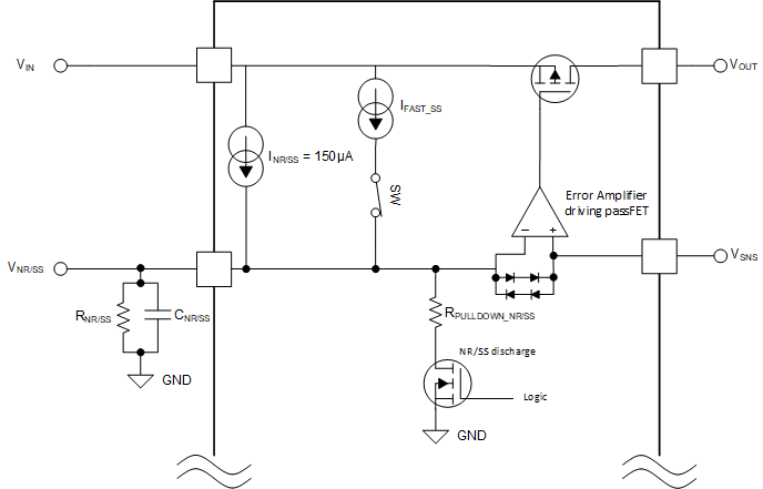
Figure 7-1 shows a simplified regulation circuit, where the input signal (VNR/SS) is generated by the internal current source (INR/SS) and the external resistor (RNR/SS). Because the error amplifier is always operating in unity-gain configuration, the LDO output voltage is directly programmed by the NR/SS pin voltage (VNR/SS). The VNR/SS reference voltage is generated by an internal low-noise current source driving the RNR/SS resistor and is designed to have very low bandwidth at the input to the error amplifier through the use of a low-pass filter (CNR/SS || RNR/SS).

This unity-gain configuration, along with the highly accurate INR/SS reference current, enables the device to achieve excellent output voltage accuracy. However, the RNR/SS accuracy can become the limiting factor when operating at low output voltage. The low-dropout voltage (VDO) provides reduced thermal dissipation and achieves robust performance. This combination of features makes this device an excellent voltage source for powering sensitive analog low-voltage devices.