-
TPS7B4253-Q1 300-mA 40-V Low-Dropout Voltage-Tracking LDO With 4-mV Tracking Tolerance
- 1 Features
- 2 Applications
- 3 Description
- 4 Revision History
- 5 Pin Configuration and Functions
- 6 Specifications
-
7 Detailed Description
- 7.1 Overview
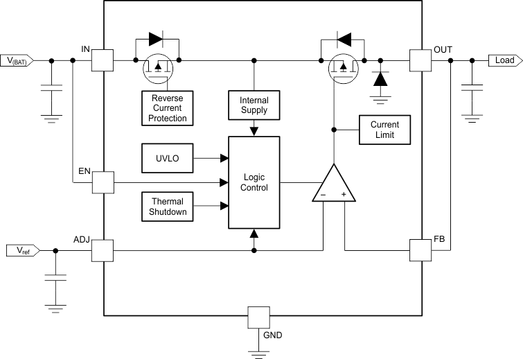
- 7.2 Functional Block Diagram
- 7.3 Feature Description
- 7.4 Device Functional Modes
- 8 Application and Implementation
- 9 Power Supply Recommendations
- 10Layout
- 11Device and Documentation Support
- 12Mechanical, Packaging, and Orderable Information
- IMPORTANT NOTICE
パッケージ・オプション
メカニカル・データ(パッケージ|ピン)
サーマルパッド・メカニカル・データ
発注情報
TPS7B4253-Q1 300-mA 40-V Low-Dropout Voltage-Tracking LDO With 4-mV Tracking Tolerance
1 Features
- Qualified for Automotive Applications
- AEC-Q100 Qualified With the Following Results:
- Device Temperature Grade 1: –40°C to +125°C Ambient Operating Temperature Range
- Device HBM ESD Classification Level 3A
- Device CDM ESD Classification Level C6
- –40 to 45-V Wide Input-Voltage Range (Maximum)
- Output Voltage Adjusts Down to:
- 1.5 to 40 V (HTSSOP)
- 2 to 40 V (SO PowerPAD™)
- 300-mA Output Current Capability
- Very-Low Output Tracking Tolerance, ±4 mV
- 320-mV Low Dropout Voltage when IOUT = 200 mA
- Separate Pins for Enable and Tracking Inputs (HTSSOP only)
- Low Quiescent Current (IQ):
- < 4 µA when EN = LOW
- 60 µA (Typical) at Light Loads
- Extremely Wide ESR Range.
- Stable With 10- to 500-µF Ceramic Output Capacitor, ESR 1 mΩ to 20 Ω
- Reverse Polarity Protection
- Current-Limit and Thermal-Shutdown Protection
- Output Short-Circuit Proof to Ground and Supply
- Inductive Clamp at OUT Pin
- Available in the Following Packages:
- 8-Pin SO PowerPAD Package
- 20-Pin HTSSOP Package
2 Applications
- Off-Board Sensor Supply
- High-Precision Voltage Tracking
- Power Switch for Off-Board Load
3 Description
For automotive off-board sensors and small current off-board modules, the power supply is through a long cable from the main board. In such cases, protection is required in the power devices for the off-board loads to prevent the onboard components from damage during a short to GND or short to battery caused by a broken cable. Off-board sensors require consistent power supply as onboard components to secure high accuracy of data acquisition.
The TPS7B4253-Q1 device is designed for automotive applications with a 45-V load dump. The device can either be used as one tracking low-dropout (LDO) regulator or voltage tracker to build one closed power loop for off-board sensors with an onboard main supply. The output of the device is accurately regulated by a reference voltage at the ADJ pin.
To provide an accurate power supply to the off-board modules, the device offers a 4-mV ultralow tracking tolerance between the ADJ and FB pins across temperature. The back-to-back PMOS topology eliminates the need for an external diode under reverse polarity condition. The TPS7B4253-Q1 device also includes thermal shutdown, inductive clamp, overload, and short-to-battery protection to prevent damage to onboard components during extreme conditions.
Device Information(1)
| PART NUMBER | PACKAGE | BODY SIZE (NOM) |
|---|---|---|
| TPS7B4253-Q1 | SO PowerPAD (8) | 4.89 mm × 3.90 mm |
| HTSSOP (20) | 6.50 mm × 4.40 mm |
- For all available packages, see the orderable addendum at the end of the data sheet.
Typical Application Schematic

4 Revision History
Changes from B Revision (January 2016) to C Revision
- Changed the following parameters in the Recommended Operating Conditions table to show values for HTSSOP and SO PowerPAD packages: VADJ, VFB, and VOUT Go
- Corrected the Functional Block DiagramGo
- Added the HTSSOP package as the example for the Application With Output Voltage Equal to the Reference Voltage sectionGo
- Corrected the Output Voltage Equals the Reference Voltage figureGo
- Added the Receiving Notification of Documentation Updates section Go
Changes from A Revision (August 2015) to B Revision
- Changed the note for the reference voltage minus the input voltage parameter in the Absolute Maximum Ratings table Go
- Added values for the SO PowerPAD package for the adjust signal valid parameters in the Electrical Characteristics tableGo
- Changed the test condition for the adjust high signal valid parameter in the Electrical Characteristics tableGo
Changes from * Revision (January 2015) to A Revision
- Changed the device status from Product Preview to Production DataGo
5 Pin Configuration and Functions
Pin Functions
| PIN | TYPE(1) | DESCRIPTION | ||
|---|---|---|---|---|
| NAME | SO PowerPAD | HTSSOP | ||
| ADJ | 5 | 11 | I | Connect the reference to this pin. A low signal disables the device and a high signal enables the device. The reference voltage can be connected directly or by a voltage divider for lower output voltages. To compensate for line influences, connect a capacitor close to the device pins. |
| EN | — | 19 | I | This pin is the enable pin. The device goes to the STANDBY state when the enable pin goes lower than the threshold value. |
| FB | 4 | 10 | I | This pin is the feedback pin which can connect to the external resistor divider to select the output voltage. |
| GND | 3 | 6 | G | Ground reference |
| 6 | 15 | |||
| IN | 8 | 20 | I | This pin is the device supply. To compensate for line influences, connect a capacitor close to the device pins. |
| NC | 2 | 2 | NC | Not connected |
| 3 | ||||
| 4 | ||||
| 5 | ||||
| 7 | ||||
| 8 | ||||
| 9 | ||||
| 7 | 12 | |||
| 13 | ||||
| 14 | ||||
| 16 | ||||
| 17 | ||||
| 18 | ||||
| OUT | 1 | 1 | O | Block to GND with a capacitor close to the device pins with respect to the capacitance and ESR requirements listed in the Output Capacitor section. |
| Exposed thermal pad | — | Connect the thermal pad to the GND pin or leave it floating. | ||
6 Specifications
6.1 Absolute Maximum Ratings
over operating free-air temperature range (unless otherwise noted)(1)| MIN | MAX | UNIT | ||
|---|---|---|---|---|
| Unregulated input voltage | IN(2)(3) | –40 | 45 | V |
| Enable input voltage | Enable input voltage(2)(3) | –40 | 45 | V |
| Regulated output voltage | Regulated output voltage(2)(4) | –1 | 45 | V |
| Voltage difference between the input and output | IN – OUT | –40 | 45 | V |
| Reference voltage | ADJ(2)(3) | –0.3 | 45 | V |
| Feedback input voltage for the tracker | FB(2)(3) | –1 | 45 | V |
| Reference voltage minus the input voltage | ADJ – IN(5) | 18 | V | |
| Operating junction temperature, TJ | –40 | 150 | °C | |
| Storage temperature, Tstg | –65 | 150 | °C | |
6.2 ESD Ratings
| VALUE | UNIT | ||||
|---|---|---|---|---|---|
| V(ESD) | Electrostatic discharge | Human body model (HBM), per AEC Q100-002(1) | NC pins | ±2000 | kV |
| All pins except for NC pins | ±4000 | kV | |||
| Charged device model (CDM), per AEC Q100-011 | ±1000 | kV | |||
6.3 Recommended Operating Conditions
over operating free-air temperature range (unless otherwise noted)(1)| MIN | MAX | UNIT | |||
|---|---|---|---|---|---|
| VIN | Unregulated input voltage(2) | 4 | 40 | V | |
| VEN | Enable input voltage | 0 | 40 | V | |
| VADJ | Adjust and enable input voltage | HTSSOP package | 1.5 | 18 | V |
| SO PowerPAD package | 2 | 18 | |||
| VFB | Feedback input voltage for the tracker | HTSSOP package | 1.5 | 18 | V |
| SO PowerPAD package | 2 | 18 | |||
| VOUT | Output voltage | HTSSOP package | 1.5 | 40 | V |
| SO PowerPAD package | 2 | 40 | |||
| C(OUT) | Output capacitor requirements(3) | 10 | 500 | µF | |
| Output ESR requirements(4) | 0.001 | 20 | Ω | ||
| TJ | Operating junction temperature range | –40 | 150 | °C | |
6.4 Thermal Information
| THERMAL METRIC(1) | TPS7B4253-Q1 | UNIT | ||
|---|---|---|---|---|
| DDA (SO PowerPAD) | PWP (HTSSOP) | |||
| 8 PINS | 20 PINS | |||
| RθJA | Junction-to-ambient thermal resistance | 45.4 | 45.9 | °C/W |
| RθJC(top) | Junction-to-case (top) thermal resistance | 51.1 | 29.2 | °C/W |
| RθJB | Junction-to-board thermal resistance | 27 | 24.7 | °C/W |
| ψJT | Junction-to-top characterization parameter | 8.2 | 1.3 | °C/W |
| ψJB | Junction-to-board characterization parameter | 26.9 | 24.5 | °C/W |
| RθJC(bot) | Junction-to-case (bottom) thermal resistance | 6.4 | 3.7 | °C/W |
6.5 Electrical Characteristics
VIN = 13.5 V, VADJ ≥ 1.5 V for HTSSOP, VADJ ≥ 2 V for SO PowerPAD, VEN ≥ 2 V, TJ = –40ºC to 150ºC unless otherwise stated| PARAMETER | TEST CONDITIONS | MIN | TYP | MAX | UNIT | ||
|---|---|---|---|---|---|---|---|
| VI(UVLO) | IN undervoltage detection | VIN rising | 3.65 | V | |||
| VIN falling | 2.8 | V | |||||
| ΔVO | Output voltage tracking accuracy(1) | IOUT = 100 µA to 300 mA, VIN = 4 to 40 V VADJ < VIN – 1 V 1.5 V < VADJ < 18 V for HTSSOP 2 V < VADJ < 18 V for SO PowerPAD |
–4 | 4 | mV | ||
| ΔVO(ΔIO) | Load regulation steady-state | IOUT = 0.1 to 300 mA, VADJ= 5 V | 4 | mV | |||
| ΔVO(ΔVI) | Line regulation steady-state | IOUT= 10 mA, VIN = 6 to 40 V, VADJ = 5 V | 4 | mV | |||
| PSRR | Power supply ripple rejection | ƒrip = 100 Hz, Vrip = 0.5 VPP, C(OUT) = 10 µF, IOUT = 100 mA | 70 | dB | |||
| V(DROPOUT) | Dropout voltage (V(DROPOUT) = VIN – VOUT) |
IOUT = 200 mA, VIN = VADJ ≥ 4 V(2) | 320 | 520 | mV | ||
| IO(lim) | Output current limitation | VADJ = 5 V, OUT short to GND | 301 | 450 | 520 | mA | |
| IR(IN) | Reverse current at IN | VIN = 0 V, VOUT = 40 V, VADJ = 5 V | –2 | 0 | µA | ||
| IR(–IN) | Reverse current at negative IN | VIN = –40 V, VOUT = 0 V, VADJ = 5 V | –10 | 0 | µA | ||
| TSD | Thermal shutdown temperature | TJ increases because of power dissipation generated by the IC | 175 | °C | |||
| TSD_hys | Thermal shutdown hysteresis | 15 | °C | ||||
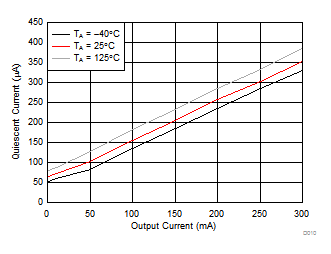
| IQ | Current consumption | 4 V ≤ VIN ≤ 40 V, VADJ = 0 V; VEN = 0 V | 2 | 4 | µA | ||
| 4 V ≤ VIN ≤ 40 V, VEN ≥ 2 V, VADJ < 0.8 V | 7 | 18 | |||||
| 4 V ≤ VIN ≤ 40 V, IOUT < 100 µA, VADJ = 5 V | 60 | 100 | |||||
| 4 V ≤ VIN ≤ 40 V, IOUT < 300 mA, VADJ = 5V | 350 | 400 | |||||
| IQ(DROPOUT) | Current consumption in dropout region | VIN = VADJ = 5 V, IOUT = 100 µA | 70 | 140 | µA | ||
| II(ADJ) | Adjust input current | VADJ = VFB = 5 V | HTSSOP package | 0.5 | µA | ||
| SO PowerPAD package | 5.5 | ||||||
| V(ADJ_LOW) | Adjust low signal valid | VOUT = 0 V | HTSSOP package | 0 | 0.8 | V | |
| SO PowerPAD package | 0 | 0.7 | |||||
| V(ADJ_HIGH) | Adjust high signal valid | |VOUT – VADJ| < 4 mV | HTSSOP package | 1.5 | 18 | V | |
| SO PowerPAD package | 2 | 18 | |||||
| V(EN_LOW) | Enable low signal valid | VOUT = 0 V | 0 | 0.7 | V | ||
| V(EN_HIGH) | Enable high Signal Valid | OUT settled | 2 | 40 | V | ||
| IEN | Enable pulldown current | 2V < VEN < 40 V | 5 | µA | |||
| IFB | FB bias current | VADJ = VFB = 5 V | 0.5 | µA | |||
6.6 Typical Characteristics
VIN = 14 V, VADJ = 5 V, VFB = VOUT, unless otherwise specified


| VIN = VADJ = 4 V | IOUT = 200 mA |

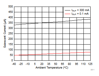

| C(OUT) = 10 µF | IOUT = 1 mA | TA = 25°C |

| VFB = VOUT | ||


| VIN = 40 to 6 V | VADJ = 5 V | C(OUT) = 10 µF |
| IOUT = 100 mA, 20 µs/div | ||
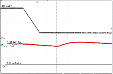
| VIN = 40 to 6 V | VADJ = 5 V | C(OUT) = 10 µF |
| IOUT = 10 mA, 20 µs/div | ||
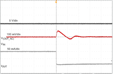
| VIN = 14 V | VADJ = 5 V | C(OUT) = 10 µF | ||
| IOUT = 100 to 10 mA, 40 µs/div | ||||


| VIN = VADJ = 4 V | ||


| VADJ = VEN = 5 V | ||

| C(OUT) = 10 µF | IOUT = 100 mA | TA = 25°C |

| VFB < VOUT | ||

| VIN = 6 to 40 V | VADJ = 5 V | C(OUT) = 10 µF |
| IOUT = 100 mA, 20 µs/div | ||

| VIN = 6 to 40 V | VADJ = 5 V | C(OUT) = 10 µF |
| IOUT = 10 mA, 20 µs/div | ||

| VIN = 14 V | VADJ = 5 V | C(OUT) = 10 µF |
| IOUT = 10 to 100 mA, 40 µs/div | ||
7 Detailed Description
7.1 Overview
The TPS7B4253-Q1 device is a monolithic integrated low-dropout voltage tracker with an ultralow tracking tolerance. Key protection circuits are integrated in the device, including output current limitation, reverse polarity protection, inductive load clamp, output short-to-battery protection, and thermal shutdown in case of an overtemperature event.
7.3 Feature Description
7.3.1 Short Circuit and Overcurrent Protection
The TPS7B4253-Q1 device features integrated fault protection which makes the device ideal for automotive applications. To keep the device in a safe area of operation during certain fault conditions, internal current-limit protection is used to limit the maximum output current. This protection protects the device from excessive power dissipation. For example, during a short-circuit condition on the output, the current through the pass element is limited to IO(lim) to protect the device from excessive power dissipation.
7.3.2 Integrated Inductive Clamp Protection
During output turnoff, the cable inductance continues to source the current from the output of the device. The device integrates an inductive clamp at the OUT pin to help to dissipate the inductive energy stored in the cable. An internal diode is connected between the OUT and GND pins with a DC-current capability of 600 mA for inductive clamp protection.
7.3.3 OUT Short to Battery and Reverse Polarity Protection
The TPS7B4253-Q1 device can withstand a short to battery when the output is shorted to the battery, as shown in Figure 22. Therefore, no damage to the device occurs.
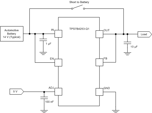 Figure 22. OUT Short to Battery, VIN = V(BAT)
A short to the battery can also occur when the device is powered by an isolated supply at lower voltage, as shown in Figure 23. In this case, the TPS7B4253-Q1 supply-input voltage is set to 7 V when a short to battery (14 V typical) occurs on the OUT pin which operates at 5 V. The internal back-to-back PMOS remains on for 1 ms during which the input voltage of the TPS7B4253-Q1 device charges up to the battery voltage. A diode connected between the output of the DC-DC converter and the input of the TPS7B4253-Q1 device is required in case the other loads connected behind the DC-DC converter cannot withstand the voltage of an automotive battery. To achieve a lower dropout voltage, TI recommends using a Schottky diode. This diode can be eliminated if the output of the DC-DC converter and the loads connect behind it withstand automotive battery voltage.
The internal back-to-back PMOS is switched to OFF when reverse polarity or short to battery occur for 1 ms. After that, the reverse current flows out through the IN pin with less than 10 µA. In the meanwhile, a special ESD structure implemented at the input ensures the device can withstand –40 V.
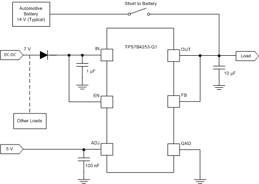 Figure 23. OUT Short to Battery, VIN < V(BAT)
In most cases, the output of the TPS7B4253-Q1 device is shorted to the battery through an automotive cable. The parasitic inductance on the cable results in LC oscillation at the output of the TPS7B4253-Q1 device when the short to battery occurs. Ideally, the peak voltage at the output of the TPS7B4253-Q1 device should be lower than the absolute-maximum voltage rating (45 V) during LC oscillation.
7.3.4 Undervoltage Shutdown
The device has an internally fixed undervoltage-shutdown threshold. Undervoltage shutdown activates when the input voltage on IN drops below UVLO. This activation ensures the regulator is not latched into an unknown state during a low input-supply voltage. If the input voltage has a negative transient that drops below the UVLO threshold and then recovers, the regulator shuts down and then powers up with a standard power-up sequence when the input voltage is above the required levels.
7.3.5 Thermal Protection
The device incorporates a thermal shutdown (TSD) circuit as a protection from overheating. During continuous normal operation, the junction temperature should not exceed the TSD trip point. If the junction temperature exceeds the TSD trip point, the output turns off. When the junction temperature decreases to 15°C (typical) lower than the TSD trip point, the output turns on.
NOTE
The purpose of the design of the internal protection circuitry of the TPS7B4253-Q1 device is to protect against overload conditions and is not intended as a replacement for proper heat-sinking. Continuously running the device into thermal shutdown degrades device reliability.
7.3.6 Regulated Output (OUT)
The OUT pin is the regulated output based on the required voltage. The output has current limitation. During initial power up, the regulator has an incorporated soft-start feature to control the initial current through the pass element.
7.3.7 Enable (EN)
The EN pin is a high-voltage-tolerant pin. A high input on the EN pin acitvates the device and turns on the regulator. The device consumes a maximum of shutdown current 4 µA when the EN pin is low. The EN pin has a maximum internal pulldown of 5 µA.
7.3.8 Adjustable Output Voltage (FB and ADJ)
7.3.8.1 OUT Voltage Equal to the Reference Voltage
With the reference voltage applied directly at the ADJ pin and the FB pin connected to the OUT pin, the voltage at the OUT pin equals to the reference voltage at the ADJ pin, as shown in Figure 24.

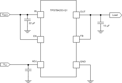 Figure 24. OUT Voltage Equal to the Reference Voltage
7.3.8.2 OUT Voltage Higher Than Reference Voltage
By using an external resistor divider connected between the OUT and FB pins, an output voltage higher than reference voltage can be generated as shown in Figure 25. Use Equation 2 to calculate the value of the output voltage. The recommended range for R1 and R2 is from 10 kΩ to 100 kΩ.

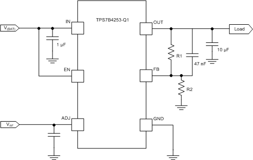 Figure 25. OUT Voltage Higher Than the Reference Voltage
7.3.8.3 Output Voltage Lower Than Reference Voltage
By using an external resistor divider connected at the ADJ pin, an output voltage lower than reference voltage can be generated as shown in Figure 26. Use Equation 3 to calculate the output voltage. The recommended value for both R1 and R2 is less than 100 kΩ.

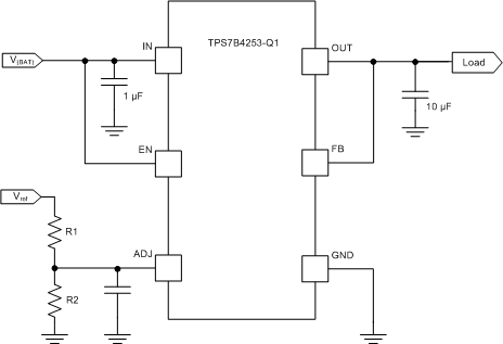 Figure 26. OUT Voltage Lower Than the Reference Voltage
7.4 Device Functional Modes
7.4.1 Operation With VIN < 4 V
The maximum UVLO voltage is 3.65 V, and the device generally operates at an input voltage above 4 V. The device can also operate at a lower input voltage; no minimum UVLO voltage is specified. At an input voltage below the actual UVLO voltage, the device does not operate.
7.4.2 Operation With EN Control
The enable rising edge threshold is 2 V (maximum). With the EN pin held above that voltage and the input voltage above 4 V, the device becomes active. The falling edge of the EN pin is 0.7 V (minimum). Holding the EN pin below that voltage disables the device, thus reducing the quiescent current of the device.
8 Application and Implementation
NOTE
Information in the following applications sections is not part of the TI component specification, and TI does not warrant its accuracy or completeness. TI’s customers are responsible for determining suitability of components for their purposes. Customers should validate and test their design implementation to confirm system functionality.
8.1 Application Information
The TPS7B4253-Q1 device is a 300-mA low-dropout tracking regulator with ultralow tracking tolerance. The PSpice transient model is available for download on the product folder and can be used to evaluate the basic function of the device.
8.2 Typical Application
8.2.1 Application With Output Voltage Equal to the Reference Voltage
Figure 27 shows the typical application circuit for the TPS7B4253-Q1 device (using the HTSSOP package as an example). Different values of external components can be used depending on the end application. An application may require a larger output capacitor during fast load steps to prevent a large drop on the output voltage. TI recommends using a low-ESR ceramic capacitor with a dielectric of type X5R or X7R.
8.2.1.1 Design Requirements
For this design example, use the parameters listed in Table 1 as the design parameters.
Table 1. Design Parameters
| DESIGN PARAMETER | EXAMPLE VALUE |
|---|---|
| Input voltage | 4 to 40 V |
| Output voltage | 1.5 to 40 V |
| Enable voltage | 2 to 40 V |
| ADJ voltage | 1.5 to 18 V |
| Output capacitor | 10 to 500 µF |
| Output capacitor ESR range | 0.001 to 20 Ω |
8.2.1.2 Detailed Design Procedure
To begin the design process, determine the following:
- Input voltage range
- Output voltage
- Reference voltage
- Output current
- Current limit
8.2.1.2.1 Input Capacitor
The device requires an input decoupling capacitor, the value of which depends on the application. The typical recommended value for the decoupling capacitor is 2.2 µF. The voltage rating must be greater than the maximum input voltage.
8.2.1.2.2 Output Capacitor
To ensure the stability of the TPS7B4253-Q1 device, the device requires an output capacitor with a value in the range from 10 µF to 500 µF and with an ESR range from 0.001 Ω to 20 Ω when the FB pin is directly connected to the OUT pin. TI recommends selecting a ceramic capacitor with low ESR to improve the load transient response.
To achieve an output voltage higher than the reference voltage, a resistor divider is connected between the OUT pin and the FB pin. In this case, a 47-nF feed forward capacitor must be connected between the OUT and FB pins for loop stability. The ESR of the output capacitor must be from 0.001 Ω to 10 Ω.
When multiple capacitors (two or more) are connected in parallel at the OUT pin, the ESR range of each output capacitor must be from 0.001 Ω to 3 Ω for loop stability.
In case the FB pin is shorted to ground, the TPS7B4253-Q1 device functions as a power switch with no need for the output capacitor.
8.2.1.3 Application Curve

| VIN = 6 to 40 V | VADJ = 5 V | C(OUT) = 10 µF | ||
| IOUT = 100 mA, 20 µs/div | ||||
8.2.2 High-Side Switch Configuration
As shown in Figure 29, by connecting the FB pin to the GND pin, the TPS7B4253-Q1 device can be used as a high-side switch with current-limit, thermal shutdown, output short-to-battery, and reverse polarity protection. The switching on and off of the device is then controlled through the EN and ADJ pins.
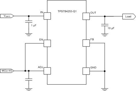 Figure 29. High-Side Switch Application
8.2.3 High Accuracy LDO
With an accurate voltage rail, the TPS7B4253-Q1 device can be used as an LDO with ultrahigh-accuracy output voltage by configuring the device as shown in Figure 30.
 Figure 30. High-Accuracy LDO Application
For example, assume the reference voltage is a 5-V rail with 0.5% accuracy. Because the tracking accuracy between the ADJ and OUT pins is specified below 4 mV across temperature, the output accuracy of the TPS7B4253-Q1 device can be calculated with Equation 4.

