SLVSCP3C January 2015 – July 2016 TPS7B4253-Q1
PRODUCTION DATA.
- 1 Features
- 2 Applications
- 3 Description
- 4 Revision History
- 5 Pin Configuration and Functions
- 6 Specifications
-
7 Detailed Description
- 7.1 Overview
- 7.2 Functional Block Diagram
- 7.3 Feature Description
- 7.4 Device Functional Modes
- 8 Application and Implementation
- 9 Power Supply Recommendations
- 10Layout
- 11Device and Documentation Support
- 12Mechanical, Packaging, and Orderable Information
パッケージ・オプション
メカニカル・データ(パッケージ|ピン)
サーマルパッド・メカニカル・データ
発注情報
7 Detailed Description
7.1 Overview
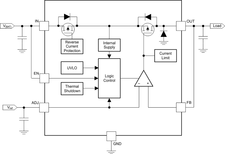
The TPS7B4253-Q1 device is a monolithic integrated low-dropout voltage tracker with an ultralow tracking tolerance. Key protection circuits are integrated in the device, including output current limitation, reverse polarity protection, inductive load clamp, output short-to-battery protection, and thermal shutdown in case of an overtemperature event.
7.3 Feature Description
7.3.1 Short Circuit and Overcurrent Protection
The TPS7B4253-Q1 device features integrated fault protection which makes the device ideal for automotive applications. To keep the device in a safe area of operation during certain fault conditions, internal current-limit protection is used to limit the maximum output current. This protection protects the device from excessive power dissipation. For example, during a short-circuit condition on the output, the current through the pass element is limited to IO(lim) to protect the device from excessive power dissipation.
7.3.2 Integrated Inductive Clamp Protection
During output turnoff, the cable inductance continues to source the current from the output of the device. The device integrates an inductive clamp at the OUT pin to help to dissipate the inductive energy stored in the cable. An internal diode is connected between the OUT and GND pins with a DC-current capability of 600 mA for inductive clamp protection.
7.3.3 OUT Short to Battery and Reverse Polarity Protection
The TPS7B4253-Q1 device can withstand a short to battery when the output is shorted to the battery, as shown in Figure 22. Therefore, no damage to the device occurs.
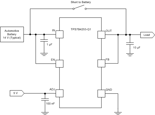 Figure 22. OUT Short to Battery, VIN = V(BAT)
A short to the battery can also occur when the device is powered by an isolated supply at lower voltage, as shown in Figure 23. In this case, the TPS7B4253-Q1 supply-input voltage is set to 7 V when a short to battery (14 V typical) occurs on the OUT pin which operates at 5 V. The internal back-to-back PMOS remains on for 1 ms during which the input voltage of the TPS7B4253-Q1 device charges up to the battery voltage. A diode connected between the output of the DC-DC converter and the input of the TPS7B4253-Q1 device is required in case the other loads connected behind the DC-DC converter cannot withstand the voltage of an automotive battery. To achieve a lower dropout voltage, TI recommends using a Schottky diode. This diode can be eliminated if the output of the DC-DC converter and the loads connect behind it withstand automotive battery voltage.
The internal back-to-back PMOS is switched to OFF when reverse polarity or short to battery occur for 1 ms. After that, the reverse current flows out through the IN pin with less than 10 µA. In the meanwhile, a special ESD structure implemented at the input ensures the device can withstand –40 V.
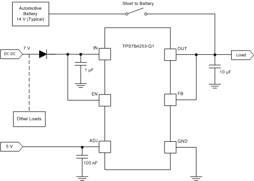 Figure 23. OUT Short to Battery, VIN < V(BAT)
In most cases, the output of the TPS7B4253-Q1 device is shorted to the battery through an automotive cable. The parasitic inductance on the cable results in LC oscillation at the output of the TPS7B4253-Q1 device when the short to battery occurs. Ideally, the peak voltage at the output of the TPS7B4253-Q1 device should be lower than the absolute-maximum voltage rating (45 V) during LC oscillation.
7.3.4 Undervoltage Shutdown
The device has an internally fixed undervoltage-shutdown threshold. Undervoltage shutdown activates when the input voltage on IN drops below UVLO. This activation ensures the regulator is not latched into an unknown state during a low input-supply voltage. If the input voltage has a negative transient that drops below the UVLO threshold and then recovers, the regulator shuts down and then powers up with a standard power-up sequence when the input voltage is above the required levels.
7.3.5 Thermal Protection
The device incorporates a thermal shutdown (TSD) circuit as a protection from overheating. During continuous normal operation, the junction temperature should not exceed the TSD trip point. If the junction temperature exceeds the TSD trip point, the output turns off. When the junction temperature decreases to 15°C (typical) lower than the TSD trip point, the output turns on.
NOTE
The purpose of the design of the internal protection circuitry of the TPS7B4253-Q1 device is to protect against overload conditions and is not intended as a replacement for proper heat-sinking. Continuously running the device into thermal shutdown degrades device reliability.
7.3.6 Regulated Output (OUT)
The OUT pin is the regulated output based on the required voltage. The output has current limitation. During initial power up, the regulator has an incorporated soft-start feature to control the initial current through the pass element.
7.3.7 Enable (EN)
The EN pin is a high-voltage-tolerant pin. A high input on the EN pin acitvates the device and turns on the regulator. The device consumes a maximum of shutdown current 4 µA when the EN pin is low. The EN pin has a maximum internal pulldown of 5 µA.
7.3.8 Adjustable Output Voltage (FB and ADJ)
7.3.8.1 OUT Voltage Equal to the Reference Voltage
With the reference voltage applied directly at the ADJ pin and the FB pin connected to the OUT pin, the voltage at the OUT pin equals to the reference voltage at the ADJ pin, as shown in Figure 24.

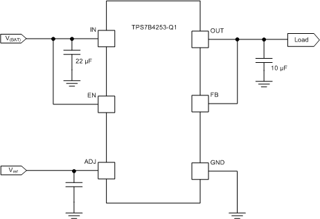 Figure 24. OUT Voltage Equal to the Reference Voltage
7.3.8.2 OUT Voltage Higher Than Reference Voltage
By using an external resistor divider connected between the OUT and FB pins, an output voltage higher than reference voltage can be generated as shown in Figure 25. Use Equation 2 to calculate the value of the output voltage. The recommended range for R1 and R2 is from 10 kΩ to 100 kΩ.

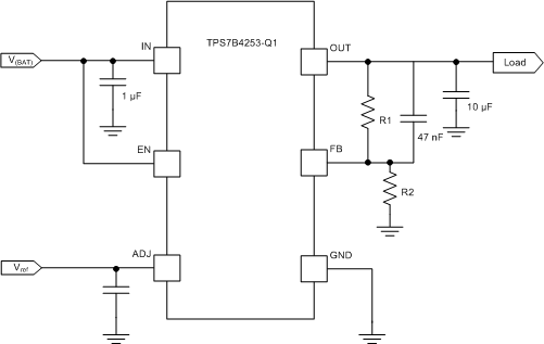 Figure 25. OUT Voltage Higher Than the Reference Voltage
7.3.8.3 Output Voltage Lower Than Reference Voltage
By using an external resistor divider connected at the ADJ pin, an output voltage lower than reference voltage can be generated as shown in Figure 26. Use Equation 3 to calculate the output voltage. The recommended value for both R1 and R2 is less than 100 kΩ.

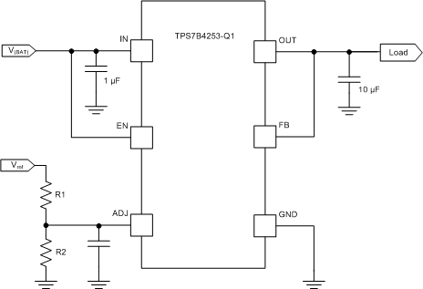 Figure 26. OUT Voltage Lower Than the Reference Voltage
7.4 Device Functional Modes
7.4.1 Operation With VIN < 4 V
The maximum UVLO voltage is 3.65 V, and the device generally operates at an input voltage above 4 V. The device can also operate at a lower input voltage; no minimum UVLO voltage is specified. At an input voltage below the actual UVLO voltage, the device does not operate.
7.4.2 Operation With EN Control
The enable rising edge threshold is 2 V (maximum). With the EN pin held above that voltage and the input voltage above 4 V, the device becomes active. The falling edge of the EN pin is 0.7 V (minimum). Holding the EN pin below that voltage disables the device, thus reducing the quiescent current of the device.
