JAJSRB5A September   2023  – November 2023 TPS7B4256-Q1

PRODUCTION DATA  

  1.   1
  2. 特長
  3. アプリケーション
  4. 概要
  5. Pin Configuration and Functions
  6. Specifications
    1. 5.1 Absolute Maximum Ratings
    2. 5.2 ESD Ratings
    3. 5.3 Recommended Operating Conditions
    4. 5.4 Thermal Information
    5. 5.5 Electrical Characteristics
    6. 5.6 Typical Characteristics
  7. Detailed Description
    1. 6.1 Overview
    2. 6.2 Functional Block Diagram
    3. 6.3 Feature Description
      1. 6.3.1 Tracker Output Voltage (VOUT)
        1. 6.3.1.1 Output Voltage Equal to Reference Voltage
        2. 6.3.1.2 Output Voltage Less Than the Reference Voltage
        3. 6.3.1.3 Output Voltage Larger Than the Reference Voltage
      2. 6.3.2 Reverse Current Protection
      3. 6.3.3 Undervoltage Lockout
      4. 6.3.4 Thermal Protection
      5. 6.3.5 Current Limit
      6. 6.3.6 Output Short to Battery
      7. 6.3.7 Tracking Regulator With an Enable Circuit
    4. 6.4 Device Functional Modes
      1. 6.4.1 Normal Operation
      2. 6.4.2 Dropout Operation
      3. 6.4.3 Operation With VIN < 3 V
      4. 6.4.4 Disable With ADJ/EN Control
  8. Application and Implementation
    1. 7.1 Application Information
      1. 7.1.1 Dropout Voltage
      2. 7.1.2 Reverse Current
    2. 7.2 Typical Application
      1. 7.2.1 Design Requirements
      2. 7.2.2 Detailed Design Procedure
        1. 7.2.2.1 Input and Output Capacitor Selection
        2. 7.2.2.2 Feedback Resistor Selection
        3. 7.2.2.3 Feedforward Capacitor
      3. 7.2.3 Application Curves
    3. 7.3 Power Supply Recommendations
    4. 7.4 Layout
      1. 7.4.1 Layout Guidelines
        1. 7.4.1.1 Package Mounting
        2. 7.4.1.2 Board Layout Recommendations to Improve PSRR and Noise Performance
        3. 7.4.1.3 Power Dissipation and Thermal Considerations
        4. 7.4.1.4 Thermal Performance Versus Copper Area
        5. 7.4.1.5 Layout Examples
  9. Device and Documentation Support
    1. 8.1 Device Support
      1. 8.1.1 Device Nomenclature
    2. 8.2 ドキュメントの更新通知を受け取る方法
    3. 8.3 サポート・リソース
    4. 8.4 Trademarks
    5. 8.5 静電気放電に関する注意事項
    6. 8.6 用語集
  10. Revision History
  11. 10Mechanical, Packaging, and Orderable Information

パッケージ・オプション

メカニカル・データ(パッケージ|ピン)
サーマルパッド・メカニカル・データ
発注情報

Thermal Performance Versus Copper Area

The most used thermal resistance parameter RθJA is highly dependent on the heat-spreading capability built into the particular PCB design, and therefore varies according to the total copper area, copper weight, and location of the planes. The RθJA recorded in the Thermal Information table is determined by the JEDEC standard (Figure 7-8), PCB, and copper-spreading area, and is only used as a relative measure of package thermal performance. For a well-designed thermal layout, RθJA is actually the sum of the package junction-to-case (bottom) thermal resistance (RθJCbot) plus the thermal resistance contribution by the PCB copper.
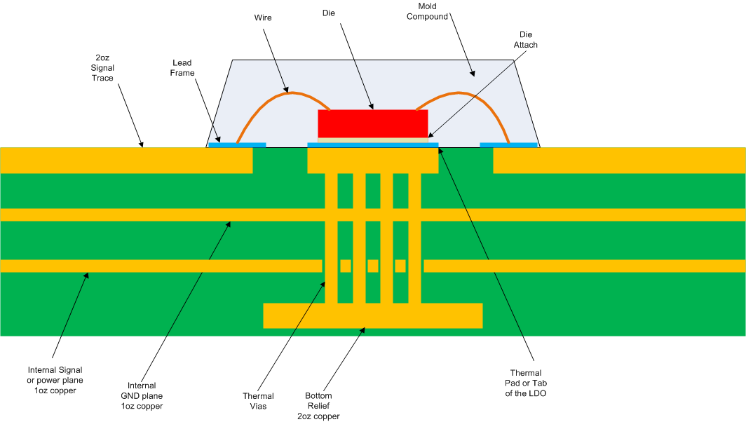
GUID-2BF2C0B9-4F00-41EC-AD78-3CA4192C654F-low.gif Figure 7-8 JEDEC Standard 2s2p PCB