JAJSD18C February 2017 – December 2022
PRODUCTION DATA
- 1 特長
- 2 アプリケーション
- 3 概要
- 4 Revision History
- 5 Pin Configuration and Functions
- 6 Specifications
-
7 Detailed Description
- 7.1 Overview
- 7.2 Functional Block Diagram
- 7.3
Feature Description
- 7.3.1 Device Enable (EN)
- 7.3.2 Adjustable Power-Good Threshold (PG, PGADJ)
- 7.3.3 Adjustable Power-Good Delay Timer (DELAY)
- 7.3.4 Undervoltage Shutdown
- 7.3.5 Current Limit
- 7.3.6 Thermal Shutdown
- 7.3.7
Integrated Watchdog
- 7.3.7.1 Window Watchdog (WTS, ROSC, FSEL and WRS)
- 7.3.7.2 Standard Watchdog (WTS, ROSC and FSEL)
- 7.3.7.3 Watchdog Service Signal and Watchdog Fault Outputs (WD and WDO)
- 7.3.7.4 ROSC Status Detection (ROSC)
- 7.3.7.5 Watchdog Enable (PG and WD_EN)
- 7.3.7.6 Watchdog Initialization
- 7.3.7.7 Window Watchdog Operation (WTS = Low)
- 7.3.7.8 Standard Watchdog Operation (WTS = High)
- 7.4 Device Functional Modes
- 8 Application and Implementation
- 9 Device and Documentation Support
- 10Mechanical, Packaging, and Orderable Information
パッケージ・オプション
メカニカル・データ(パッケージ|ピン)
- PWP|16
サーマルパッド・メカニカル・データ
- PWP|16
発注情報
7.3.7.8 Standard Watchdog Operation (WTS = High)
The standard watchdog is able to monitor whether the frequency of the watchdog service signal (WD) is lower than a certain value. A watchdog low-voltage fault is reported when the frequency of the watchdog service signal is lower than the set value.
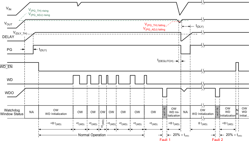
Figure 7-5 shows the standard watchdog initialization and operation for the TPS7B63xx-Q1. Similar to the window watchdog, after output the voltage is in regulation and PG asserts high, the standard watchdog becomes enabled when an external signal pulls WD_EN low. This causes the standard watchdog to initialize and wait for a service signal during the first initialization window for 8 times the duration of t(WD). A service signal applied to the WD pin during the first open window resets the watchdog counter and another open window starts. To prevent a fault condition from occurring, watchdog service must occur during the every open window to prevent a fault condition from occurring. The fault output (WDO), externally pulled up to VOUT (typical), stays high as long as the watchdog receives proper service and there is not fault condition.
 Figure 7-5 Standard Watchdog Operation
Two different fault conditions occur in Figure 7-5:
- Fault 1: The watchdog service signal is not received during the open window. WDO is triggered after the maximum open-window duration t(WD).
- Fault 2: The watchdog service signal is not received during the WD initialization. WDO is triggered after the maximum initialization window duration 8 × t(WD).