JAJSKF7A December 2020 – April 2021 TPS7B87-Q1
PRODUCTION DATA
- 1 特長
- 2 アプリケーション
- 3 概要
- 4 Revision History
- 5 Pin Configuration and Functions
- 6 Specifications
- 7 Detailed Description
- 8 Application and Implementation
- 9 Power Supply Recommendations
- 10Layout
- 11Device and Documentation Support
- 12Mechanical, Packaging, and Orderable Information
パッケージ・オプション
メカニカル・データ(パッケージ|ピン)
サーマルパッド・メカニカル・データ
発注情報
5 Pin Configuration and Functions
Figure 5-1 KVU
Package,5-Pin TO-252,Top View
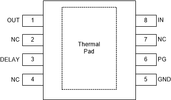
 Figure 5-2 DDA
Package,8-Pin HSOIC,Top View
Figure 5-2 DDA
Package,8-Pin HSOIC,Top ViewTable 5-1 Pin Functions
| PIN | TYPE(1) | DESCRIPTION | ||
|---|---|---|---|---|
| NAME | KVU | DDA | ||
| DELAY | 4 | 3 | I | Power-good delay adjustment pin. Connect a capacitor from this pin to GND to set the PG reset delay. Leave this pin floating for a default (t(DLY_FIX)) delay. See the Section 7.3.1 section for more information. If this functionality is not desired, leave this pin floating because connecting this pin to GND causes a permanent increase in the GND current. |
| GND | 3 | 5 | G | Ground reference |
| NC | — | 2, 4, 7 | — | No internal connection. This pin can be left floating or tied to GND for best thermal performance. |
| PG | 2 | 6 | I | Power-good pin. This pin has an internal pullup resistor. Do not connect this pin to VOUT or any other biased voltage rail. VPG is logic level high when VOUT is above the power-good threshold. See the Section 7.3.1 section for more information. |
| IN | 1 | 8 | P | Input power-supply voltage pin. For best transient response and to minimize input impedance, use the recommended value or larger ceramic capacitor from IN to GND as listed in the Recommended Operating Conditions table and the Section 8.2.2.1 section. Place the input capacitor as close to the input of the device as possible. |
| OUT | 5 | 1 | O | Regulated output voltage pin. A capacitor is required from OUT to GND for stability. For best transient response, use the nominal recommended value or larger ceramic capacitor from OUT to GND; see the Recommended Operating Conditions table and the Section 8.2.2.2 section. Place the output capacitor as close to output of the device as possible. If using a high equivalent series resistance (ESR) capacitor, decouple the output with a 100-nF ceramic capacitor. |
| Thermal pad | Pad | Pad | — | Connect the thermal pad to a large area GND plane for improved thermal performance. |
(1) I = input; O = output; P = power; G = ground.