JAJSD99A April 2017 – August 2017 TPS7H1101A-SP
PRODUCTION DATA.
5 Pin Configuration and Functions
HKR Package
16-Pin CFP
Bottom View
Pin Functions
| PIN | I/O | DESCRIPTION | |
|---|---|---|---|
| NAME | NO. | ||
| SS | 1 | I/O | Soft-start terminal. Connecting an external capacitor slows down the output voltage ramp rate after enable event. |
| EN | 2 | I | Enable terminal. Driving this terminal to logic high enables the device; driving the terminal to logic low disables the device. |
| VIN | 3 | I | Unregulated supply voltage. TI recommends to connect an input capacitor as a good analog circuit practice. |
| 4 | |||
| 5 | |||
| 6 | |||
| PCL | 7 | I/O | Programmable current limit. A resistor to GND sets the overcurrent limit activation point. The range of resistor that can be used on the PCL terminal to GND is 8.2 kΩ to 160 kΩ. |
| GND | 8 | — | Ground/thermal pad.(1) |
| PG/OC | 9 | O | Power Good terminal. PG is an open-drain output to indicate the output voltage reaches 90% of target. PG terminal is also used as indicator when an overcurrent condition is activated. PG pin should have a pull-up resistor to the VOUT pin. |
| CS | 10 | I/O | Current sense terminal. Resistor connected from CS to VIN. CS terminal indicates voltage proportional to output current. CS terminal low: Foldback current limit disabled. CS terminal high: Foldback current limit enabled. |
| VOUT | 11 | O | Regulated output. |
| 12 | |||
| 13 | |||
| 14 | |||
| COMP | 15 | I/O | Internal compensation point for error amplifier. |
| FB | 16 | I | The output voltage feedback input through voltage dividers. See the Adjustable Output Voltage (Feedback Circuit) section. |
(1) Thermal pad must be connected to GND.
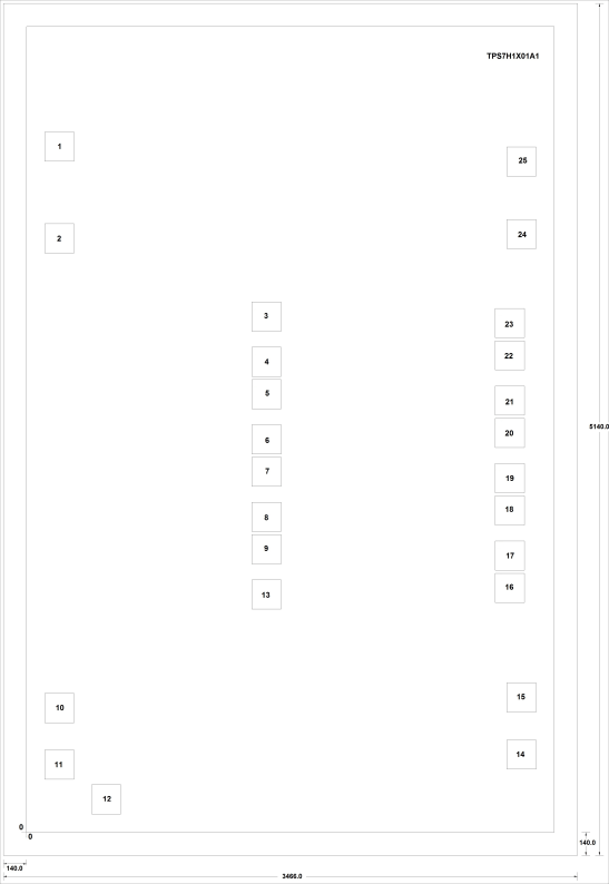
Bare Die Information
| DIE THICKNESS | BACKSIDE FINISH | BACKSIDE POTENTIAL | BOND PAD METALLIZATION COMPOSITION |
BOND PAD THICKNESS |
|---|---|---|---|---|
| 15 mils | Silicon with backgrind | Ground | AlCu | 30 kA |

NOTE:
All dimensions are in microns.Bond Pad Coordinates in Microns
| DESCRIPTION | PAD NUMBER | X MIN | Y MIN | X MAX | Y MAX |
|---|---|---|---|---|---|
| SS | 1 | 109.89 | 4046.805 | 287.19 | 4224.105 |
| EN | 2 | 109.89 | 3493.35 | 287.19 | 3670.65 |
| VIN | 3 | 1359.99 | 3021.345 | 1537.29 | 3198.645 |
| VIN | 4 | 1359.99 | 2749.005 | 1537.29 | 2926.305 |
| VIN | 5 | 1359.99 | 2553.705 | 1537.29 | 2731.005 |
| VIN | 6 | 1359.99 | 2281.365 | 1537.29 | 2458.665 |
| VIN | 7 | 1359.99 | 2086.065 | 1537.29 | 2263.365 |
| VIN | 8 | 1359.99 | 1813.725 | 1537.29 | 1991.025 |
| VIN | 9 | 1359.99 | 1618.425 | 1537.29 | 1795.725 |
| PCL | 10 | 109.89 | 660.285 | 287.19 | 837.585 |
| GND | 11 | 109.89 | 319.455 | 287.19 | 496.755 |
| GND | 12 | 392.58 | 109.935 | 569.88 | 287.235 |
| VIN | 13 | 1359.99 | 1346.085 | 1537.29 | 1523.385 |
| PG/OC | 14 | 2898.945 | 379.62 | 3076.245 | 556.92 |
| CS | 15 | 2898.945 | 724.32 | 3076.245 | 901.62 |
| VOUT | 16 | 2829.105 | 1384.695 | 3006.405 | 1561.995 |
| VOUT | 17 | 2829.105 | 1579.815 | 3006.405 | 1757.115 |
| VOUT | 18 | 2829.105 | 1852.335 | 3006.405 | 2029.635 |
| VOUT | 19 | 2829.105 | 2047.455 | 3006.405 | 2224.755 |
| VOUT | 20 | 2829.105 | 2319.975 | 3006.405 | 2497.275 |
| VOUT | 21 | 2829.105 | 2515.095 | 3006.405 | 2692.395 |
| VOUT | 22 | 2829.105 | 2787.615 | 3006.405 | 2964.915 |
| VOUT | 23 | 2829.105 | 2982.735 | 3006.405 | 3160.035 |
| COMP | 24 | 2898.945 | 3519.72 | 3076.245 | 3697.02 |
| FB | 25 | 2898.945 | 3956.535 | 3076.245 | 4133.835 |