JAJSKK6A November 2020 – December 2021 TPS7H4010-SEP
PRODUCTION DATA
- 1 特長
- 2 アプリケーション
- 3 概要
- 4 Revision History
- 5 Pin Configuration and Functions
- 6 Specifications
-
7 Detailed Description
- 7.1 Overview
- 7.2 Functional Block Diagram
- 7.3
Feature Description
- 7.3.1 Synchronous Step-Down Regulator
- 7.3.2 Auto Mode and FPWM Mode
- 7.3.3 Fixed-Frequency Peak Current-Mode Control
- 7.3.4 Adjustable Output Voltage
- 7.3.5 Enable and UVLO
- 7.3.6 Internal LDO, VCC_UVLO, and BIAS Input
- 7.3.7 Soft Start and Voltage Tracking
- 7.3.8 Adjustable Switching Frequency
- 7.3.9 Frequency Synchronization and Mode Setting
- 7.3.10 Internal Compensation and CFF
- 7.3.11 Bootstrap Capacitor and VBOOT-UVLO
- 7.3.12 Power-Good and Overvoltage Protection
- 7.3.13 Overcurrent and Short-Circuit Protection
- 7.3.14 Thermal Shutdown
- 7.4 Device Functional Modes
-
8 Application and Implementation
- 8.1 Application Information
- 8.2
Typical Application
- 8.2.1 Design Requirements
- 8.2.2
Detailed Design Procedure
- 8.2.2.1 Output Voltage Setpoint
- 8.2.2.2 Switching Frequency
- 8.2.2.3 Input Capacitors
- 8.2.2.4 Inductor Selection
- 8.2.2.5 Output Capacitor Selection
- 8.2.2.6 Feed-Forward Capacitor
- 8.2.2.7 Bootstrap Capacitors
- 8.2.2.8 VCC Capacitor
- 8.2.2.9 BIAS
- 8.2.2.10 Soft Start
- 8.2.2.11 Undervoltage Lockout Setpoint
- 8.2.2.12 PGOOD
- 8.2.3 Application Curves
- 9 Power Supply Recommendations
- 10Layout
- 11Device and Documentation Support
- 12Mechanical, Packaging, and Orderable Information
パッケージ・オプション
デバイスごとのパッケージ図は、PDF版データシートをご参照ください。
メカニカル・データ(パッケージ|ピン)
- RNP|30
- KGD|0
サーマルパッド・メカニカル・データ
- RNP|30
発注情報
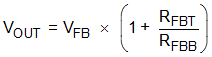
8.2.2.1 Output Voltage Setpoint
The output voltage of the TPS7H4010-SEP device is externally adjustable using a resistor divider network. The divider network is comprised of top feedback resistor RFBT and bottom feedback resistor RFBB. Use Equation 24 to determine the output voltage of the converter.
Typically, RFBT = 10 kΩ to 100 kΩ is recommended. Larger RFBT and RFBB values reduce the quiescent current going through the divider, which help maintain high efficiency at very light loads. But larger divider values also make the feedback path more susceptible to noise. If efficiency at very light loads is critical in a certain application, RFBT up to 1 MΩ can be used.

RFBT = 100 kΩ is selected here. RFBB = 24.99 kΩ can be calculated to get 5-V output voltage.