SLVSAD1B June 2010 – January 2016 TPS80010
PRODUCTION DATA.
- 1 Features
- 2 Applications
- 3 Description
- 4 Revision History
- 5 Pin Configuration and Functions
- 6 Specifications
- 7 Detailed Description
- 8 Application and Implementation
- 9 Power Supply Recommendations
- 10Layout
- 11Device and Documentation Support
- 12Mechanical, Packaging, and Orderable Information
パッケージ・オプション
メカニカル・データ(パッケージ|ピン)
- RSM|32
サーマルパッド・メカニカル・データ
- RSM|32
発注情報
8 Application and Implementation
NOTE
Information in the following applications sections is not part of the TI component specification, and TI does not warrant its accuracy or completeness. TI’s customers are responsible for determining suitability of components for their purposes. Customers should validate and test their design implementation to confirm system functionality.
8.1 Application Information
The TPS80010 is ideal for dual-cell alkaline battery-powered and noise-sensitive applications. The application controller has the ability to enable resources on the power management IC to allow for maximum flexibility. The device resources are often used to power memory, IO, and optical sensors. These devices are common in wireless keyboards and video game controllers.
8.2 Typical Application
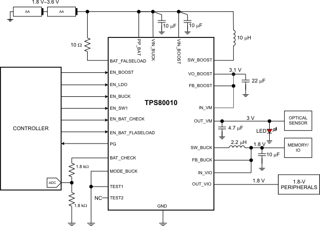 Figure 11. TPS80010 Typical Application Diagram
8.2.1 Design Requirements
The design requirements for TPS80010 are located in Table 1.
Table 1. TPS80010 Design Requirements
| RESOURCE | VOLTAGE |
|---|---|
| Buck | 1.8 V |
| Boost | 3.1 V |
8.2.2 Detailed Design Procedure
8.2.2.1 Buck Output Filter Design
The TPS80010 buck regulator is designed to operate with inductors in the range of 1.5 µH to 4.7 µH and with output capacitors in the range of 4.7 µF to 22 µF. The part is optimized for operation with a 2.2-µH inductor and 10-µF output capacitor.
Larger or smaller inductor values can be used to optimize the performance of the device for specific operation conditions. For stable operation, the L and C values of the output filter must not be less than 1-µH effective inductance and 3.5-µF effective capacitance.
8.2.2.2 Buck Inductor Selection
The inductor value has a direct effect on the ripple current. The selected inductor must be rated for its DC resistance and saturation current. The inductor ripple current (ΔIL) decreases with higher inductance and increases with higher VIN or VBUCK.
The inductor selection also has an impact on the output-voltage ripple in PFM mode. Higher inductor values lead to lower output-voltage ripple and higher PFM frequency; lower inductor values lead to a higher output-voltage ripple but lower PFM frequency.
Equation 1 calculates the maximum inductor current in PWM mode under static load conditions. The saturation current of the inductor must be rated higher than the maximum inductor current, as calculated with Equation 2. This is recommended because during heavy load transients, the inductor current rises above the calculated value.


where
- f = Switching frequency (2.25 MHz typical)
- L = Inductor value
- ΔIL = Peak-to-peak inductor ripple current
- ILmax = Maximum inductor current
A more conservative approach is to select the inductor current rating just for the switch current limit, ILIMF, of the converter.
Accepting larger values of ripple current allows the use of lower inductance values, but results in higher output voltage ripple, greater core losses, and lower output current capability.
The total losses of the coil have a strong impact on the efficiency of the DC-DC conversion and consist of both the losses in the DC resistance (R(DC)) and the following frequency-dependent components:
- The losses in the core material (magnetic hysteresis loss, especially at high switching frequencies)
- Additional losses in the conductor from the skin effect (current displacement at high frequencies)
- Magnetic field losses of the neighboring windings (proximity effect)
- Radiation losses
8.2.2.3 Buck Output Capacitor Selection
The advanced fast-response voltage mode control scheme of the TPS80010 buck regulator allows the use of tiny ceramic capacitors. Ceramic capacitors with low ESR values have the lowest output voltage ripple and are recommended. The output capacitor requires either an X7R or X5R dielectric. Y5V- and Z5U-dielectric capacitors, aside from their wide variation in capacitance over temperature, become resistive at high frequencies. At nominal load current, the device operates in PWM mode and the RMS ripple current is calculated with Equation 3.

At nominal load current, the device operates in PWM mode and the overall output voltage ripple is the sum of the voltage spike caused by the output capacitor ESR plus the voltage ripple caused by charging and discharging the output capacitor in Equation 4.

At light-load currents, the converter operates in power-save mode, and the output-voltage ripple depends on the output-capacitor and inductor values. Larger output-capacitor and inductor values minimize the voltage ripple in PFM mode and tighten DC output accuracy in PFM mode.
8.2.2.4 Buck Input Capacitor Selection
An input capacitor is required for best input voltage filtering and for minimizing the interference with other circuits caused by high input-voltage spikes. For most applications, a 4.7-µF to 10-µF ceramic capacitor is recommended. Because a ceramic capacitor loses up to 80% of its initial capacitance at 5 V, TI recommends that 10-µF input capacitors be used for input voltages > 4.5 V. The input capacitor can be increased without any limit for better input-voltage filtering. Take care when using only small ceramic input capacitors. When a ceramic capacitor is used at the input and the power is being supplied through long wires, such as from a wall adapter, a load step at the output or VIN step on the input can induce ringing at the VIN_BUCK pin. This ringing can couple to the output and be mistaken as loop instability or could even damage the part by exceeding the maximum ratings.
Table 2. Recommended Component List for Buck Converter
| COMPONENT | VALUE | PART | SUPPLIER | SIZE |
|---|---|---|---|---|
| Inductor | 2.2 μH | LQM2HPN2R2MJ0L | Murata | 2.5 mm × 2 mm × 1.2 mm (1008) |
| LPS3015-222ML | Coilcraft | 3 mm × 3 mm × 1.5 mm | ||
| Cacitor (IN) | 10 μF | GRM188R60J106ME47D | Murata | 0603 |
| Capacitor (OUT) | 10 μF | GRM188R60J106ME47D | Murata | 0603 |
8.2.2.5 Boost Inductor Selection
To ensure proper operation of the TPS80010 boost DC-DC converter, a suitable inductor must be connected between pins VIN_BOOST and SW_BOOST. Inductor values of 4.7 μH show good performance over the whole input and output voltage range.
Choosing other inductance values affects the switching frequency f proportional to 1/L as shown in Equation 5.

Choosing inductor values higher than 4.7 μH can improve efficiency due to reduced switching frequency and correspondingly reduced switching losses. Using inductor values less than 2.2 μH is not recommended.
Having selected an inductance value, the peak current for the inductor in steady-state operation can be calculated. Equation 6 gives the peak current estimate.

IL,MAX is the required minimum inductor-current rating. The load-transient or overcurrent conditions may require an even higher current rating.
The condition in Equation 7 provides an easy way to determine whether the device is in continuous or discontinuous operation. As long as the condition is true, the device operates in continuous-current mode. If the condition becomes false, discontinuous-current operation is established.

Due to the use of current hysteretic control in the TPS80010 boost, the series resistance of the inductor can impact the operation of the main switch. There is a simple calculation that can ensure proper operation of the TPS80010 boost converter. The relationship between the series resistance (RIN), the input voltage (VIN), and the switch current limit (ISW) is shown in Equation 8.

Examples include Equation 9 and Equation 10.

In Equation 9, RIN < 2.5 V / 400 mA; therefore, RIN must be less than 6.25 Ω.

In Equation 10, RIN < 1.8 V / 400 mA; therefore, RIN must be less than 4.5 Ω.
8.2.2.6 Boost Input Capacitor
The input capacitor must be at least 10 μF to improve transient behavior of the regulator and EMI behavior of the total power-supply circuit. The input capacitor must be a ceramic capacitor and be placed as close as possible to the VIN_BOOST and GND pins of the IC. These capacitors must be X7R or X5R ceramic capacitors.
8.2.2.7 Boost Output Capacitor
For the output capacitor COUT, TI recommends using small X7R or X5R ceramic capacitors placed as close as possible to the VO_BOOST and GND pins of the IC. If, for any reason, the application requires the use of large capacitors which cannot be placed close to the IC, the use of a small ceramic capacitor with a capacitance value of around 4.7 μF in parallel with the larger one is recommended. This small capacitor must be placed as close as possible to the VO_BOOST and GND pins of the IC.
A minimum effective capacitance value of 6 μF must be used; 10 μF is recommended. If the inductor value exceeds 4.7 μH, the value of the effective output capacitance value must be half the inductance value or higher for stability reasons; see Equation 11.

NOTE
When choosing the output capacitor, be aware of the effects of bias voltage, temperature, and tolerance on the effective capacitance of the component. A capacitor in a 0603 package size suffers more capacitance degradation than a 0805 package at a similar bias voltage. For example, either a 22-µF 0603-sized capacitor or a 10-µF 0805-sized capacitor is required to work with a nominal 10-µH inductor.
The TPS80010 boost is not sensitive to ESR in terms of stability. Using low-ESR capacitors, such as ceramic capacitors, is recommended to minimize output-voltage ripple. If heavy load changes are expected, the output capacitor value must be increased to avoid output voltage drops during fast load transients.
Table 3. Recommended Component List for Boost Converter
| COMPONENT | VALUE | PART | SUPPLIER | SIZE |
|---|---|---|---|---|
| Inductor | 10 μH | CBC3225T100MR | Taiyo Yuden | 3.2 mm × 2.5 mm × 2.5 mm (1210) |
| DO3314-103ML | Coilcraft | 3.3 mm × 3.3 mm × 1.4 mm | ||
| Capacitor (IN) | 10 μF | GRM188R60J106ME47D | Murata | 0603 |
| Capacitor (OUT) | 22 μF | AMK107BJ226MA-T | Taiyo Yuden | 0603 |
8.2.3 Application Curves
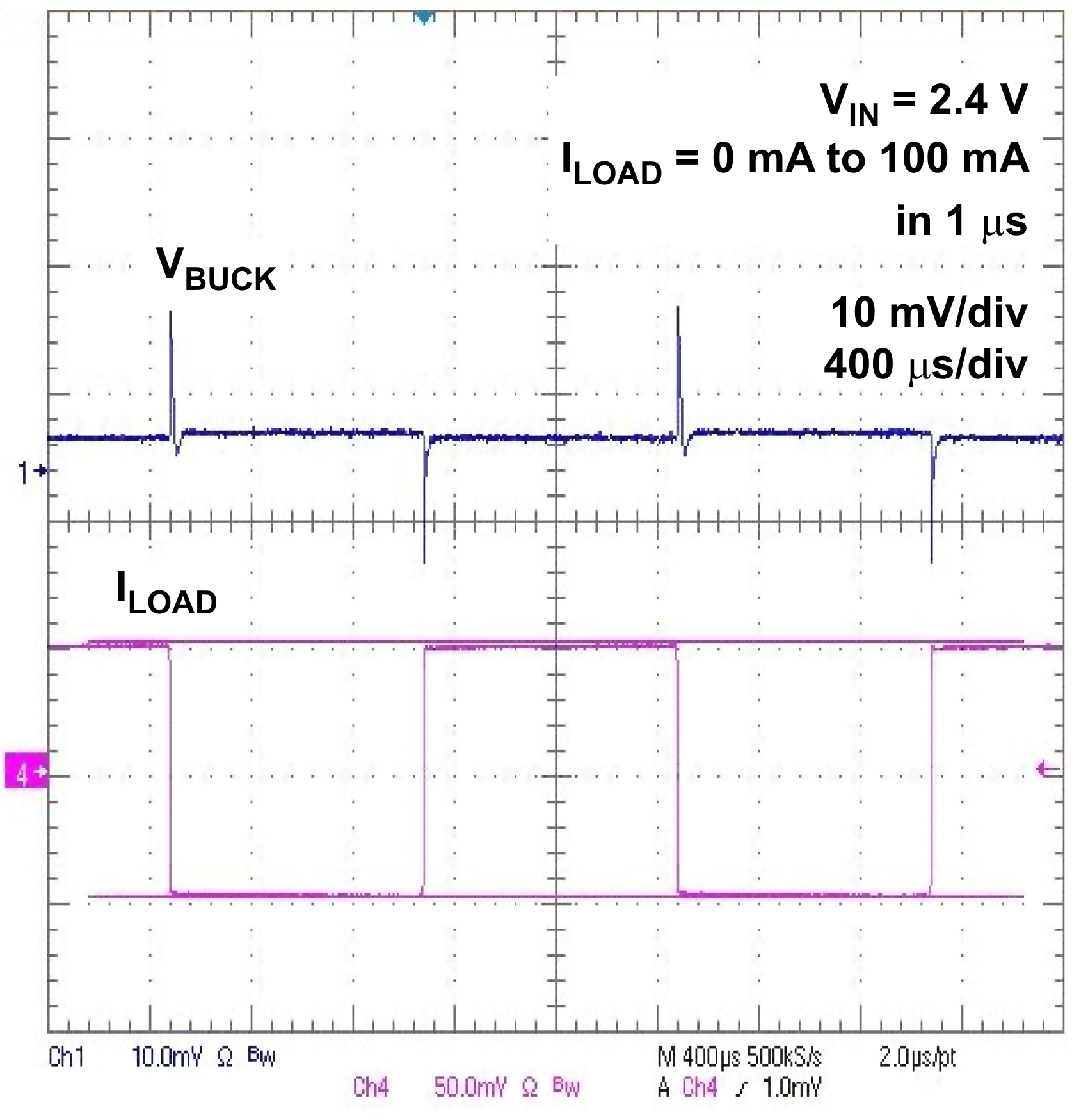 Figure 12. Buck Output Load Transient Response
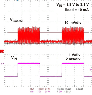 Figure 14. Boost Line Transient Response
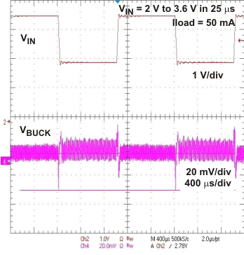 Figure 13. Buck Output Line Transient Response
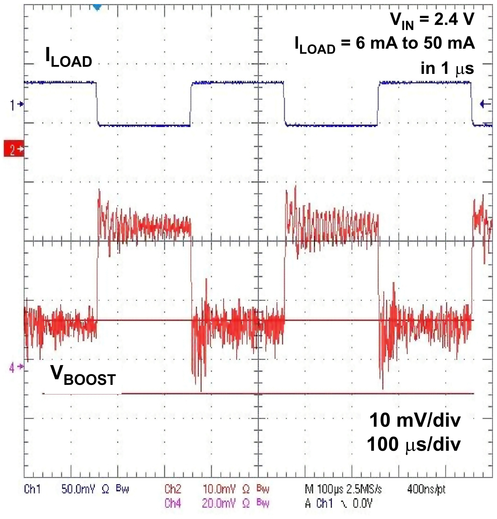 Figure 15. Boost Load Transient Response