SLVSBR0C October 2014 – June 2015 TPS8268090 , TPS8268105 , TPS8268120 , TPS8268150 , TPS8268180
PRODUCTION DATA.
- 1 Features
- 2 Applications
- 3 Description
- 4 Revision History
- 5 Device Comparison Table
- 6 Pin Configuration and Functions
- 7 Specifications
- 8 Detailed Description
- 9 Application and Implementation
- 10Power Supply Recommendations
- 11Layout
- 12Device and Documentation Support
- 13Mechanical, Packaging, and Orderable Information
パッケージ・オプション
デバイスごとのパッケージ図は、PDF版データシートをご参照ください。
メカニカル・データ(パッケージ|ピン)
- SIP|9
サーマルパッド・メカニカル・データ
発注情報
7 Specifications
7.1 Absolute Maximum Ratings
over operating free-air temperature range (unless otherwise noted) (1)| MIN | MAX | UNIT | ||
|---|---|---|---|---|
| VI | Voltage at VIN(2) | –0.3 | 6 | V |
| Voltage at VOUT(2) | –0.3 | 3.6 | ||
| Voltage at EN, MODE(2) | –0.3 | VIN + 0.3 | ||
| Peak output current | 1600 | mA | ||
| TJ | Operating internal junction temperature range | –40 | 125 | °C |
| Tstg | Storage temperature range | –55 | 125 | °C |
(1) Stresses beyond those listed under Absolute Maximum Ratings may cause permanent damage to the device. These are stress ratings only, which do not imply functional operation of the device at these or any other conditions beyond those indicated under Recommended Operating Conditions. Exposure to absolute-maximum-rated conditions for extended periods may affect device reliability.
(2) All voltage values are with respect to network ground terminal.
7.2 ESD Ratings
| VALUE | UNIT | |||
|---|---|---|---|---|
| V(ESD) | Electrostatic discharge (1)(2) | Human body model | ±2000 | V |
| Charge device model | ±500 | V | ||
| Machine model | ±100 | V |
(1) JEDEC document JEP155 states that 500-V HBM allows safe manufacturing with a standard ESD control process.
(2) JEDEC document JEP157 states that 250-V CDM allows safe manufacturing with a standard ESD control process.
7.3 Recommended Operating Conditions
over operating free-air temperature range (unless otherwise noted)| MIN | NOM | MAX | UNIT | |||
|---|---|---|---|---|---|---|
| VIN | Input voltage range | 2.5 | 5.5 | V | ||
| IOUT | Peak output current for TPS8268090, TPS8268105, TPS8268120 | VIN ≥ 2.8V | 0 | 1600(1) | mA | |
| Peak output current for TPS8268150, TPS8268180 | VIN ≥ 3.2V | |||||
| IOUT | Average output current for TPS8268090, TPS8268105, TPS8268120 | VIN ≥ 2.7V | 0 | 1200(1) | mA | |
| Average output current for TPS8268150, TPS8268180 | VIN ≥ 2.9V | |||||
| IOUT | Average output current during soft-start | Vout ≤ 0.9 x VOUT,nom | 0 | 1000(2) | mA | |
| Additional effective input capacitance | 0 | µF | ||||
| Additional effective output capacitance | 0 | 30(3) | µF | |||
| TA | Operating ambient temperature range | –40 | 85 | °C | ||
(1) See Thermal and Reliability Information for additional details
(2) See Soft Start for additional details
(3) Due to the dc bias effect of ceramic capacitors, the effective capacitance is lower then the nominal value when a voltage is applied.
7.4 Thermal Information
| THERMAL METRIC(1) | TPS8268x | UNIT | |
|---|---|---|---|
| SIP | |||
| 9 PINS | |||
| RθJA | Junction-to-ambient thermal resistance | 62 | °C/W |
| RθJC(top) | Junction-to-case (top) thermal resistance | 22 | °C/W |
| RθJB | Junction-to-board thermal resistance | 25 | °C/W |
| ψJT | Junction-to-top characterization parameter | 11 | °C/W |
| ψJB | Junction-to-board characterization parameter | 25 | °C/W |
| RθJC(bot) | Junction-to-case (bottom) thermal resistance | n/a | °C/W |
(1) For more information about traditional and new thermal metrics, see the Semiconductor and IC Package Thermal Metrics application report, SPRA953.
7.5 Electrical Characteristics
Minimum and maximum values are at VIN = 2.5 V to 5.5 V, EN = VIN and TA = –40°C to 85°C; Circuit of Parameter Measurement Information section (unless otherwise noted). Typical values are at VIN = 3.6 V, EN = VIN and TA = 25°C (unless otherwise noted).| PARAMETER | TEST CONDITIONS | MIN | TYP | MAX | UNIT | |||
|---|---|---|---|---|---|---|---|---|
| SUPPLY CURRENT | ||||||||
| IQ | Operating quiescent current | IOUT = 0mA | 7 | mA | ||||
| ISD | Shutdown current | EN = low | 0.5 | 5 | μA | |||
| UVLO | Undervoltage lockout threshold | VIN rising | 2.1 | 2.3 | V | |||
| VIN falling | 1.95 | 2.25 | V | |||||
| ENABLE, MODE | ||||||||
| VIH | High-level input voltage | 0.9 | V | |||||
| VIL | Low-level input voltage | 0.4 | V | |||||
| Ilkg | Input leakage current | Input connected to GND or VIN; TJ = –40°C to 85°C | 0.01 | 1.5 | μA | |||
| PROTECTION | ||||||||
| Thermal shutdown | Temperature rising | 140 | °C | |||||
| Thermal shutdown hysteresis | Temperature falling | 10 | °C | |||||
| ILIM | Average output current limit | 2100 | mA | |||||
| ISC | Input current limit under short-circuit condition | VOUT shorted to ground | 150 | mA | ||||
| OUTPUT | ||||||||
| TPS8268180 | 1.80 | V | ||||||
| TPS8268150 | 1.50 | V | ||||||
| TPS8268120 | 1.20 | V | ||||||
| VOUT,NOM | Nominal output voltage | TPS8268105 | 1.05 | V | ||||
| TPS8268090 | 0.90 | V | ||||||
| Output voltage accuracy | TPS8268120, TPS8268105, TPS8268090 | 2.8V ≤ VIN ≤ 5.5V, 0mA ≤ IOUT ≤ 1600 mA TJ = –40°C to 85°C |
0.985×VOUT,NOM | VOUT,NOM | 1.015×VOUT,NOM | V | ||
| TPS8268180, TPS8268150 | 3.2V ≤ VIN ≤ 5.5V, 0mA ≤ IOUT ≤ 1600 mA TJ = –40°C to 85°C |
|||||||
| TPS8268120, TPS8268105, TPS8268090 | 2.7V ≤ VIN ≤ 5.5V, 0mA ≤ IOUT ≤ 1200 mA TJ = –40°C to 125°C |
0.98×VOUT,NOM | VOUT,NOM | 1.025×VOUT,NOM | V | |||
| TPS8268180, TPS8268150 | 2.9V ≤ VIN ≤ 5.5V, 0mA ≤ IOUT ≤ 1200 mA TJ = –40°C to 125°C |
|||||||
| Line regulation | VIN = 2.5V to 5.5V, IOUT = 200 mA | 0.2 | %/V | |||||
| Load regulation | IOUT = 0mA to 1600 mA | –0.85 | %/A | |||||
| fSW | Nominal oscillator frequency | IOUT = 0mA | 5.5 | MHz | ||||
| RDIS | VOUT discharge resistor | 12 | Ω | |||||
7.6 Timing Requirements
Minimum and maximum values are at VIN = 2.5 V to 5.5 V, EN = VIN and TA = –40°C to 85°C; Circuit of Parameter Measurement Information section (unless otherwise noted). Typical values are at VIN = 3.6 V, EN = VIN and TA = 25°C (unless otherwise noted).7.7 Typical Characteristics
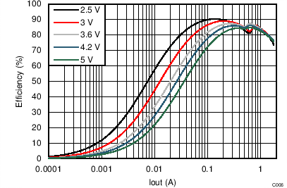
| VOUT = 1.80V | 25°C |
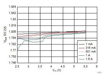
| VOUT = 1.80 V | 25°C |
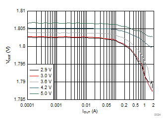
| VOUT = 1.80 V | 25°C |
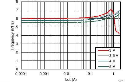
| VOUT = 1.80 V | 25°C |
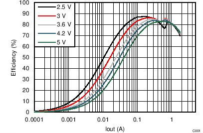
| VOUT = 1.50V | 25°C |
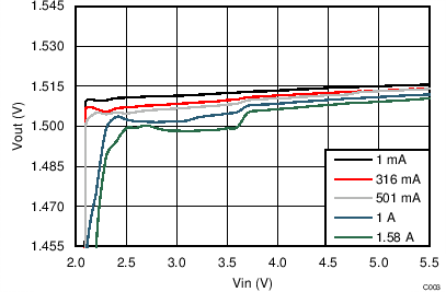
| VOUT = 1.50 V | 25°C |
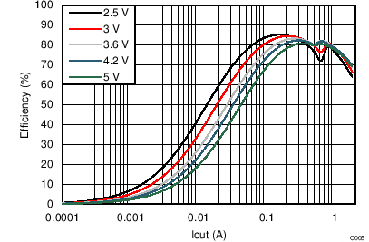
| VOUT = 1.20V | 25°C |
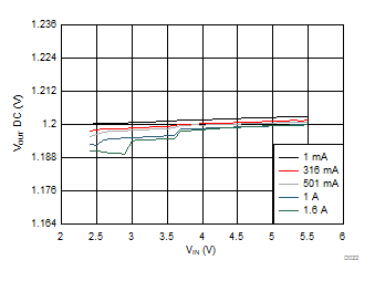
| VOUT = 1.20 V | 25°C |
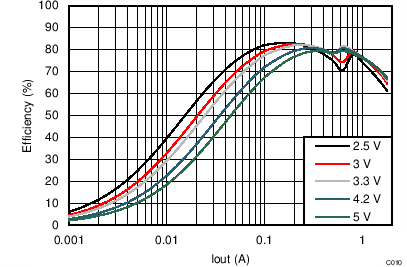
| VOUT = 1.05V | 25°C |
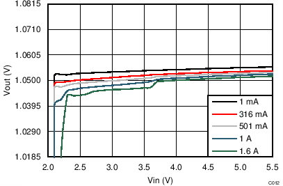
| VOUT = 1.05 V | 25°C |
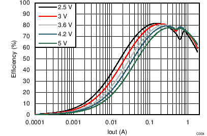
| VOUT = 0.9 V | 25°C |
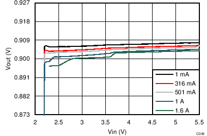
| VIN = 0.9 V | 25°C |
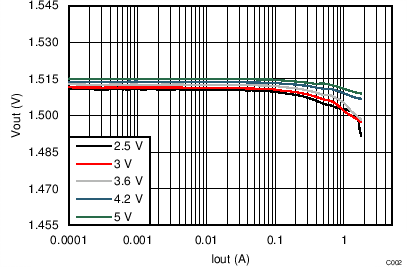
| VOUT = 1.50 V | 25°C |
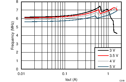
| VOUT = 1.50 V | 25°C |
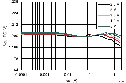
| VOUT = 1.20 V | 25°C |
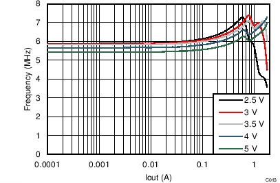
| VOUT = 1.20 V | 25°C |
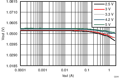
| VOUT = 1.05 V | 25°C |
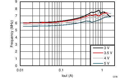
| VOUT = 1.05 V | 25°C |
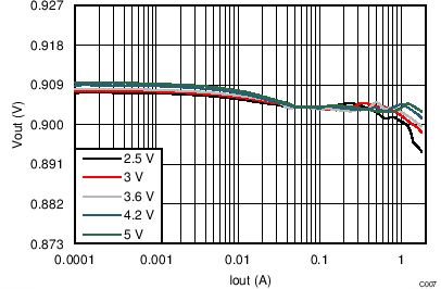
| VIN = 0.9 V | 25°C |
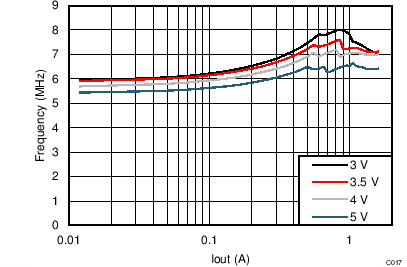
| VIN = 0.9 V | 25°C |