SLUSBZ6A April 2016 – August 2016 TPS92515 , TPS92515-Q1 , TPS92515HV , TPS92515HV-Q1
PRODUCTION DATA.
- 1 Features
- 2 Applications
- 3 Description
- 4 Revision History
- 5 Device Comparison Table
- 6 Pin Configuration and Functions
- 7 Specifications
-
8 Detailed Description
- 8.1 Overview
- 8.2 Functional Block Diagram
- 8.3
Feature Description
- 8.3.1 General Operation
- 8.3.2 Current Sense Comparator
- 8.3.3 OFF Timer
- 8.3.4 OFF-Timer, Shunt FET Dimming or Shunted Output Condition
- 8.3.5 Internal N-channel MOSFET
- 8.3.6 VCC Internal Regulator and Undervoltage Lockout (UVLO)
- 8.3.7 Analog Adjust Input
- 8.3.8 Thermal Protection
- 8.3.9 Junction Temperature Relative Estimation
- 8.3.10 BOOT and BOOT UVLO
- 8.3.11 PWM (UVLO and Enable)
- 8.4 Device Functional Modes
-
9 Application and Implementation
- 9.1 Application Information
- 9.2
Typical Application
- 9.2.1 General Design Procedure
- 9.2.2 Design Requirements
- 9.2.3
Detailed Design Procedure
- 9.2.3.1 Calculating Duty Cycle
- 9.2.3.2 Calculate OFF-Time Estimate
- 9.2.3.3 Calculate OFF-Time Resistor ROFF
- 9.2.3.4 Calculate the Inductance Value
- 9.2.3.5 Calculate the Sense Resistance
- 9.2.3.6 Calculate Input Capacitance
- 9.2.3.7 Verify Peak Current for Inductor Selection
- 9.2.3.8 Calculate Output Capacitance
- 9.2.3.9 Calculate UVLO Resistance Values
- 9.2.4 Application Curves
- 9.3 Dos and Don'ts
- 10Power Supply Recommendations
- 11Layout
- 12Device and Documentation Support
- 13Mechanical, Packaging, and Orderable Information
9.2.1.7 Calculate Output Capacitance
Because current is being regulated and is continuous, no output capacitance is required to supply the load and maintain output voltage. This regulation helps when designing a high-frequency PWM dimming on the LED load. When no output capacitor is used, the same design calculations for ΔIL-PP also apply to ΔILED-PP.
A capacitor placed in parallel with the LED load can be used to reduce ΔILED-PP while keeping the same average current through both the inductor and the LED load. With an output capacitor, the inductance can be lowered, making the magnetic smaller and less expensive. Alternatively, the circuit can be run at lower frequency with the same inductor value, improving the efficiency and increasing the maximum allowable average output voltage. A parallel output capacitor is also useful in applications where the inductor or input voltage tolerance is poor. Adding a capacitor that reduces ΔILED-PP to well below the target provides headroom for changes in inductance or VIN that might otherwise push the maximum ΔILED-PP too high.
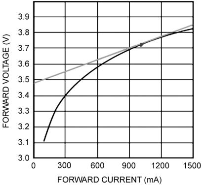
 Figure 31. Calculating Dynamic Resistance rD from LED Characteristics.
 Determine the output capacitance by establishing the desired ΔILED-PP and the LED dynamic resistance, rD. Calculate the dynamic resistance as the slope of the LED exponential DC characteristic at the nominal operating point as shown in Figure 31. Simply dividing the forward voltage by the forward current at the nominal operating point results in an incorrect value that is between 5 times and 10 times too high. Calculate total dynamic resistance for a string of n LEDs connected in series as the dynamic resistance of one device multiplied by n. Use Equation 22 and Equation 23 to estimate ΔILED-PP when using a parallel capacitor:

