SLUSBZ6A April 2016 – August 2016 TPS92515 , TPS92515-Q1 , TPS92515HV , TPS92515HV-Q1
PRODUCTION DATA.
- 1 Features
- 2 Applications
- 3 Description
- 4 Revision History
- 5 Device Comparison Table
- 6 Pin Configuration and Functions
- 7 Specifications
-
8 Detailed Description
- 8.1 Overview
- 8.2 Functional Block Diagram
- 8.3
Feature Description
- 8.3.1 General Operation
- 8.3.2 Current Sense Comparator
- 8.3.3 OFF Timer
- 8.3.4 OFF-Timer, Shunt FET Dimming or Shunted Output Condition
- 8.3.5 Internal N-channel MOSFET
- 8.3.6 VCC Internal Regulator and Undervoltage Lockout (UVLO)
- 8.3.7 Analog Adjust Input
- 8.3.8 Thermal Protection
- 8.3.9 Junction Temperature Relative Estimation
- 8.3.10 BOOT and BOOT UVLO
- 8.3.11 PWM (UVLO and Enable)
- 8.4 Device Functional Modes
-
9 Application and Implementation
- 9.1 Application Information
- 9.2
Typical Application
- 9.2.1 General Design Procedure
- 9.2.2 Design Requirements
- 9.2.3
Detailed Design Procedure
- 9.2.3.1 Calculating Duty Cycle
- 9.2.3.2 Calculate OFF-Time Estimate
- 9.2.3.3 Calculate OFF-Time Resistor ROFF
- 9.2.3.4 Calculate the Inductance Value
- 9.2.3.5 Calculate the Sense Resistance
- 9.2.3.6 Calculate Input Capacitance
- 9.2.3.7 Verify Peak Current for Inductor Selection
- 9.2.3.8 Calculate Output Capacitance
- 9.2.3.9 Calculate UVLO Resistance Values
- 9.2.4 Application Curves
- 9.3 Dos and Don'ts
- 10Power Supply Recommendations
- 11Layout
- 12Device and Documentation Support
- 13Mechanical, Packaging, and Orderable Information
3 Description
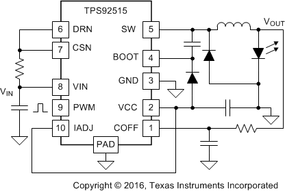
The TPS92515 family of devices are compact monolithic switching regulators integrating a low resistance N-Channel MOSFET. The devices are intended for high-brightness LED lighting applications where efficiency, high bandwidth, PWM and/or analog dimming and small size are important.
The regulator operates using a constant off-time, peak current control. The operation is simple: after an off-time based on the output voltage, an on-time begins. The on-time ends once the inductor peak current threshold is reached. The TPS92515 device can be configured to maintain a constant peak-to-peak ripple during the ON and OFF periods of a shunt FET dimming cycle. This is ideal for maintaining a linear response across the entire shunt FET dimming range.
Steady-state accuracy is aided by the inclusion of a low-offset, high-side comparator. LED current can be modulated using either Analog or PWM dimming, or both simultaneously. Other features include UVLO, wide input voltage operation, inherent LED Open operation and wide operating temperature range with thermal shut-down.
The TPS92515 and TPS92515-Q1 devices have an operational input range up to 42 V. The TPS92515HV and TPS92515HV-Q1 offer high-voltage options with an input range up to 65 V. All are available in a thermally enhanced 10-pin HVSSOP package.
Device Information(1)
| PART NUMBER | PACKAGE | BODY SIZE (NOM) |
|---|---|---|
| TPS92515 | HVSSOP (10) | 3 mm x 3 mm |
| TPS92515-Q1 | ||
| TPS92515HV | ||
| TPS92515HV-Q1 |
- For all available packages, see the orderable addendum at the end of the data sheet.
Simplified Buck LED Driver Application
