SNVS900B DECEMBER 2012 – December 2015 TPS92560
PRODUCTION DATA.
- 1 Features
- 2 Applications
- 3 Description
- 4 Revision History
- 5 Pin Configuration and Functions
- 6 Specifications
- 7 Detailed Description
- 8 Application and Implementation
- 9 Power Supply Recommendations
- 10Layout
- 11Device and Documentation Support
- 12Mechanical, Packaging, and Orderable Information
パッケージ・オプション
メカニカル・データ(パッケージ|ピン)
- DGQ|10
サーマルパッド・メカニカル・データ
- DGQ|10
発注情報
8 Application and Implementation
NOTE
Information in the following applications sections is not part of the TI component specification, and TI does not warrant its accuracy or completeness. TI’s customers are responsible for determining suitability of components for their purposes. Customers should validate and test their design implementation to confirm system functionality.
8.1 Application Information
In the applications that need true regulation of the LED current, the intrinsic input current control loop can be changed to monitor the LED current by adding an external LED current sensing circuit. Figure 18 and Figure 23 show the example circuits for true LED current regulation in boost and SEPIC configurations respectively. In the circuits, the U3 (TL431) maintains a constant 2.5-V voltage drop on the resistors, R3 and R7. Because the U2 (TL431) maintains a constant voltage drop on the R3, the power dissipation on the output current sensing resistor, R7 can be minimized by setting a low voltage drop on the R7. Because the change of the current flowing through the R7 reflects in the change of the cathode current of U3 and eventually adjusts the ADJ pin voltage of the TPS92560, the LED current is regulated independent of the change of the input voltage.
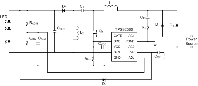 Figure 16. Typical Application Circuit of the TPS92560 Using SEPIC Configuration
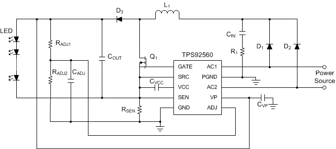 Figure 17. Typical Application Circuit of the TPS92560 Using Boost Configuration
8.2 Typical Applications
8.2.1 Boost Application Design Example
 Figure 18. TPS92560 in Boost Configuration With Input Current Regulation
8.2.1.1 Design Requirements
The specifications of the boost application circuit in Figure 18 are as listed as follows:
- Input Voltage: VIN = 12 V
- LED Stack Voltage: VLED = 21 V
- Input Current: IIN(nom) = 500 mA
- Input Power = 6 W
- overvoltage Level: VVP(OVP) = 40 V
- Switching Frequency: fSW = 1.4 MHz
8.2.1.2 Detailed Design Procedure
8.2.1.2.1 Calculate Values for the ADJ Resistors
First choose a value for RADJ2 in the range of 1 kΩ and 10 kΩ. For this example RADJ2 = 1 kΩ is chosen. Then calculate RADJ1 for the desired OVP level using Equation 25.

Choose the nearest standard resistor value of RADJ1 = 102 kΩ.
8.2.1.2.2 Calculate the Sense Voltage and Sense Resistor Value
Given the calculated ADJ resistor values the sense voltage (VSEN) can be calculated using Equation 26.

Given a current sense voltage of 206 mV the current sense resistor value (RSEN) can be calculated using Equation 27.

The nearest standard value if 0.412Ω so choose RSEN = 0.412Ω.
8.2.1.2.3 Calculate the Inductor Value
Given a desired switching frequency of 1.4 MHz the inductor value can be calculated using Equation 28.


Choose the closest standard inductor value of L = 22 µH.
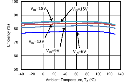
8.2.1.3 Application Curve
8.2.2 Boost Application Circuit With LED Current Regulation
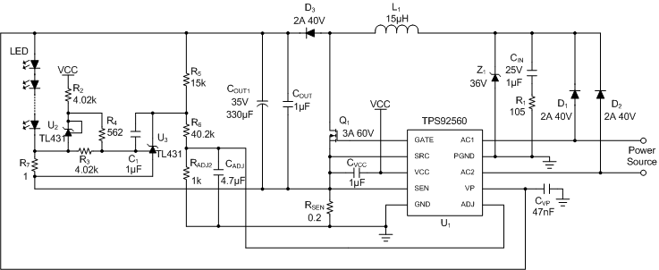 Figure 20. Using the TPS92560 in Boost Configuration With LED Current Regulation
8.2.2.1 Design Requirements
The specifications of the boost application circuit in Figure 18 are as as follows:
- Objective input voltage: 3 VDC to 18 VDC / 12 VAC( 50 Hz or 60 Hz) / Generic MR16 electronic transformer
- LED forward voltage: 20 VDC typical
- Output current: 300 mA typical (at 12-VDC input)
- Output power: 6 W typical (at 12-VDC input)
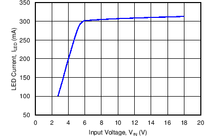
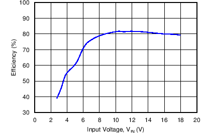
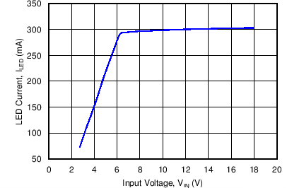
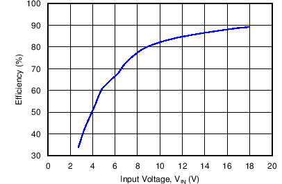
8.2.2.2 Application Curves
All curves taken at VIN = 3 V to 18 VDC in boost configuration, with 300mA nominal output current, 6 serial LEDs. TA = 25°C.
8.2.3 SEPIC Application Circuit With LED Current Regulation
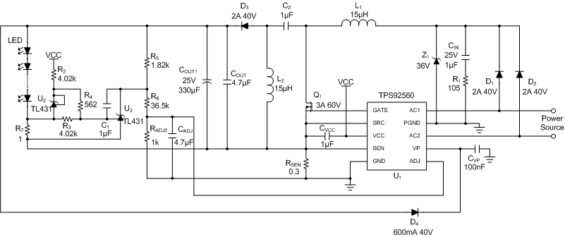 Figure 23. Using the TPS92560 in SEPIC Configuration With LED Current Regulation
8.2.3.1 Design Requirements
The specifications of the SEPIC application circuit in Figure 18 are as listed as follows:
- Objective input voltage: 3 VDC to 18 VDC / 12 VAC (50 Hz or 60 Hz) / Generic MR16 electronic transformer
- LED forward voltage: 13 VDC typical
- Output current: 300 mA typical (at 12-VDC input)
- Output power: 4 W typical (at 12-VDC input)
8.2.3.2 Application Curves
All curves taken at VIN = 3 V to 18 VDC in SEPIC configuration, with 300-mA nominal output current, 4 serial LEDs. TA = 25°C.
