JAJSH91B April   2019  – January 2020 TPS92613-Q1

PRODUCTION DATA.  

  1. 特長
  2. アプリケーション
  3. 概要
    1.     Device Images
      1.      代表的なアプリケーションの図
  4. 改訂履歴
  5. Pin Configuration and Functions
    1.     Pin Functions
  6. Specifications
    1. 6.1 Absolute Maximum Ratings
    2. 6.2 ESD Ratings
    3. 6.3 Recommended Operating Conditions
    4. 6.4 Thermal Information
    5. 6.5 Electrical Characteristics
    6. 6.6 Timing Requirements
    7. 6.7 Typical Characteristics
  7. Detailed Description
    1. 7.1 Overview
    2. 7.2 Functional Block Diagram
    3. 7.3 Feature Description
      1. 7.3.1 Power Supply
        1. 7.3.1.1 Power-On Reset (POR)
        2. 7.3.1.2 Low-Quiescent-Current
      2. 7.3.2 Constant-Current Driver
      3. 7.3.3 PWM Control
      4. 7.3.4 Supply Control
      5. 7.3.5 Diagnostics and Protection
        1. 7.3.5.1 Open-Circuit Detection
        2. 7.3.5.2 Short-to-GND Detection
        3. 7.3.5.3 Overtemperature Protection
        4. 7.3.5.4 DIAGEN
        5. 7.3.5.5 Low-Dropout Operation
      6. 7.3.6 FAULT Bus Output With One-Fails–All-Fail
      7. 7.3.7 Fault Table
    4. 7.4 Device Functional Modes
      1. 7.4.1 Undervoltage Lockout, V(SUPPLY) < V(POR_rising)
      2. 7.4.2 Normal Operation V(SUPPLY) ≥ 4.5 V
      3. 7.4.3 Low-Voltage Dropout Operation
      4. 7.4.4 Fault Mode
  8. Application and Implementation
    1. 8.1 Application Information
    2. 8.2 Typical Applications
      1. 8.2.1 Single-Channel LED Driver With Diagnostics
        1. 8.2.1.1 Design Requirements
        2. 8.2.1.2 Detailed Design Procedure
        3. 8.2.1.3 Application Curves
      2. 8.2.2 Single-Channel LED Driver With Heat Sharing
        1. 8.2.2.1 Design Requirements
        2. 8.2.2.2 Detailed Design Procedure
        3. 8.2.2.3 Application Curves
  9. Power Supply Recommendations
  10. 10Layout
    1. 10.1 Layout Guidelines
    2. 10.2 Layout Example
  11. 11デバイスおよびドキュメントのサポート
    1. 11.1 ドキュメントのサポート
      1. 11.1.1 関連資料
    2. 11.2 ドキュメントの更新通知を受け取る方法
    3. 11.3 サポート・リソース
    4. 11.4 商標
    5. 11.5 静電気放電に関する注意事項
    6. 11.6 Glossary
  12. 12メカニカル、パッケージ、および注文情報

パッケージ・オプション

メカニカル・データ(パッケージ|ピン)
サーマルパッド・メカニカル・データ
発注情報

Application Curves

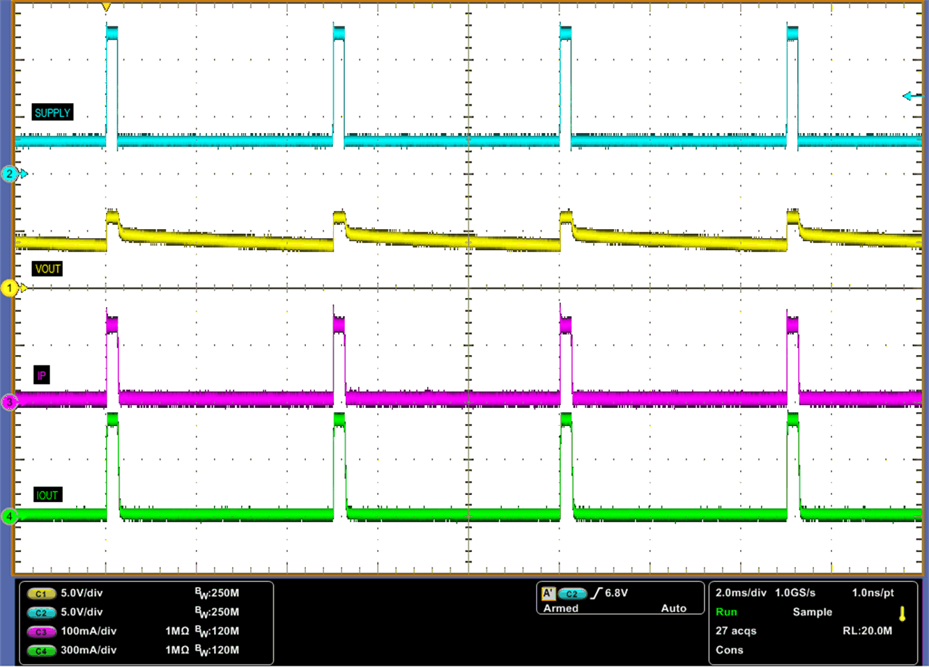
TPS92613-Q1 App-wave-05-slvsec4.gif
Ch. 1 = V(SUPPLY) Ch. 2 = V(OUT) Ch. 3 = I(P)
Ch. 4 = I(LED) F(SUPPLY) = 200 Hz Duty Cycle = 5%
V(SUPPLYHI) = 12V V(SUPPLYLO) = 2.5V
Figure 28. Pulse Supply Control Output Current (D = 5%)
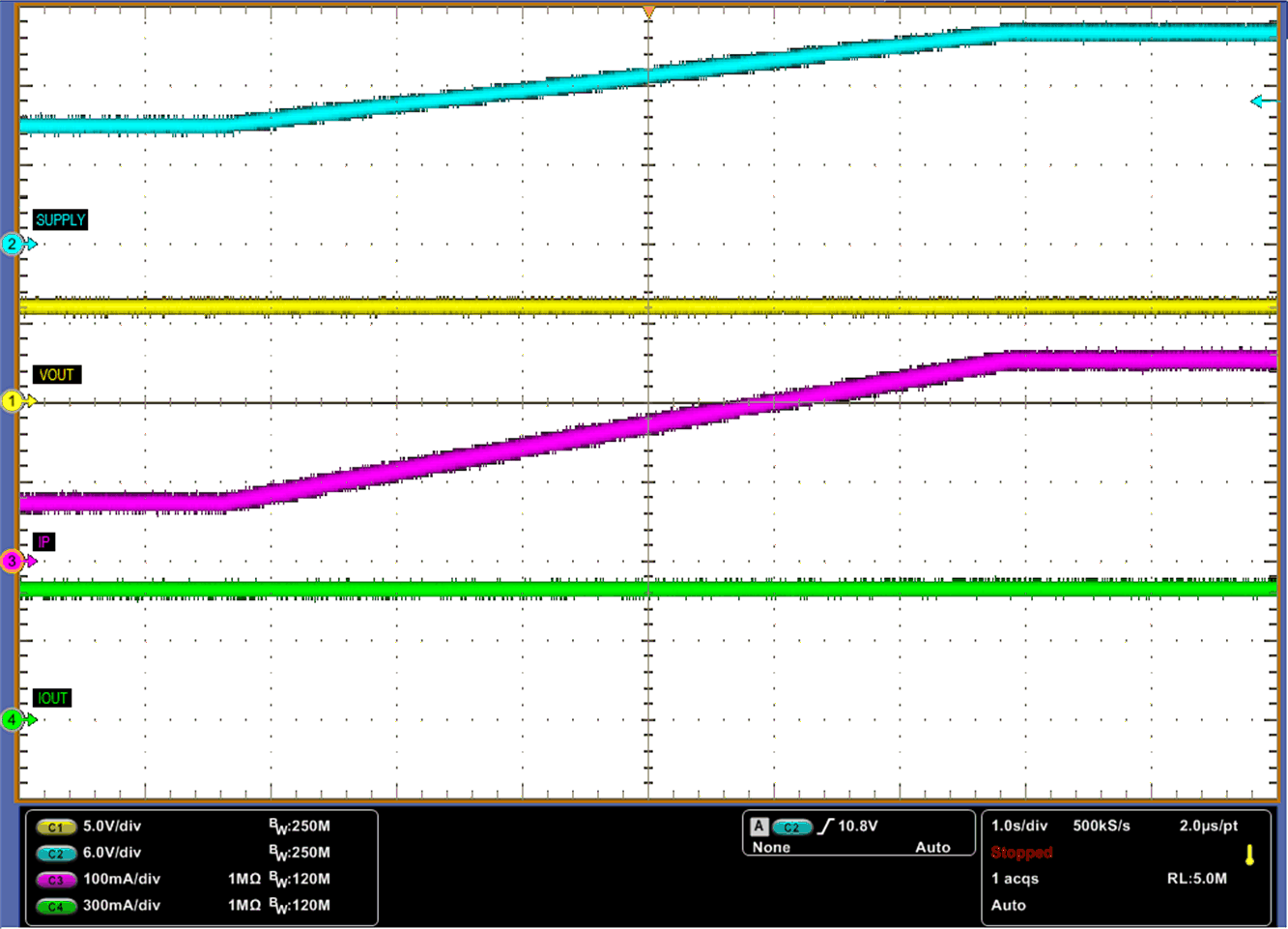
TPS92613-Q1 App-wave-03-slvsec4.gif
Ch. 1 = V(SUPPLY) Ch. 2 = V(OUT) Ch. 3 = I(P)
Ch. 4 = I(LED) V(SUPPLY) increases from 9 V to 16 V
Figure 30. Constant Output Current With Supply Voltage Increasing
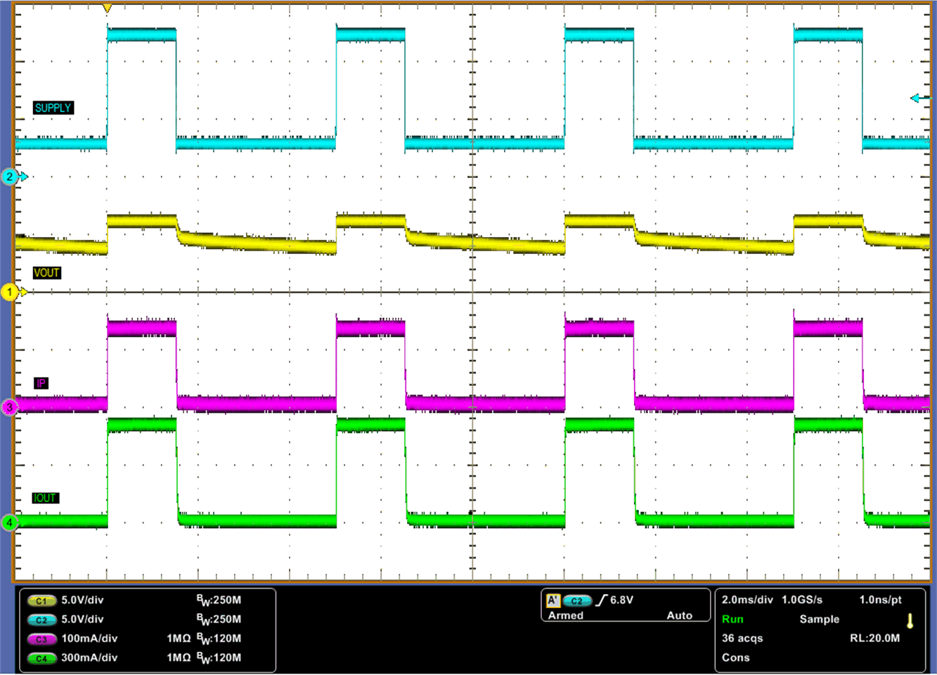
TPS92613-Q1 App-wave-04-slvsec4.gif
Ch. 1 = V(SUPPLY) Ch. 2 = V(OUT) Ch. 3 = I(P)
Ch. 4 = I(LED) F(SUPPLY) = 200 Hz Duty Cycle = 30%
V(SUPPLYHI) = 12V V(SUPPLYLO) = 2.5V
Figure 29. Pulse Supply Control Output Current (D = 30%)
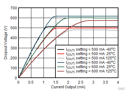
TPS92613-Q1 D007_SLVSEC4.gif
Figure 31. Output Current vs Dropout Voltage