JAJSKJ1A December 2020 – February 2021 TPS929121-Q1
PRODUCTION DATA
- 1 特長
- 2 アプリケーション
- 3 概要
- 4 Revision History
- 5 Device Comparison Table
- 6 Pin Configuration and Functions
- 7 Specifications
-
8 Detailed Description
- 8.1 Overview
- 8.2 Functional Block Diagram
- 8.3
Feature Description
- 8.3.1 Device Bias and Power
- 8.3.2 Constant Current Output
- 8.3.3 PWM Dimming
- 8.3.4 On-chip 8-bit Analog-to-Digital Converter (ADC)
- 8.3.5
Diagnostic and Protection in Normal State
- 8.3.5.1 Fault Masking
- 8.3.5.2 Supply Undervoltage Lockout Diagnostics in Normal State
- 8.3.5.3 Low-Supply Warning Diagnostics in Normal State
- 8.3.5.4 Reference Diagnostics in Normal State
- 8.3.5.5 Pre-Thermal Warning and Overtemperature Protection in Normal State
- 8.3.5.6 Communication Loss Diagnostic in Normal State
- 8.3.5.7 LED Open-Circuit Diagnostics in Normal State
- 8.3.5.8 LED Short-Circuit Diagnostics in Normal State
- 8.3.5.9 On-Demand Off-State Invisible Diagnostics
- 8.3.5.10 On-Demand Off-State Single-LED Short-Circuit (SS) Diagnostics
- 8.3.5.11 Automatic Single-LED Short-Circuit (AutoSS) Detection in Normal State
- 8.3.5.12 EEPROM CRC Error in Normal State
- 48
- 8.3.6
Diagnostic and Protection in Fail-Safe States
- 8.3.6.1 Fault Masking
- 8.3.6.2 Supply UVLO Diagnostics in Fail-Safe States
- 8.3.6.3 Low-supply Warning Diagnostics in Fail-Safe states
- 8.3.6.4 Reference Diagnostics at Fail-Safe States
- 8.3.6.5 Overtemperature Protection in Fail-Safe State
- 8.3.6.6 LED Open-circuit Diagnostics in Fail-Safe State
- 8.3.6.7 LED Short-circuit Diagnostics in Fail-Safe State
- 8.3.6.8 EEPROM CRC Error in Fail-safe State
- 58
- 8.4 Device Functional Modes
- 8.5 Programming
- 8.6 Register Maps
- 9 Application and Implementation
- 10Power Supply Recommendations
- 11Layout
- 12Device and Documentation Support
- 13Mechanical, Packaging, and Orderable Information
パッケージ・オプション
メカニカル・データ(パッケージ|ピン)
- PWP|24
サーマルパッド・メカニカル・データ
- PWP|24
発注情報
8.4.7 ERR Output
The ERR pin is a programmable fault indicator pin. It can be used as an interrupt output to master controller in case there is any fault in normal mode. In fail-safe states, the ERR pin can be used as an output to other ERR pin of other TPS929121-Q1 to realize one-fails-all-fail at system level. The ERR pin is a open-drain output with current limit up to I(pd_ERR). TI recommends a <10-kΩ external pullup resistor from the ERR pin to the same IO voltage of master controller.
In normal state, when a fault is triggered, depending on the fault type, the ERR pin is either pulled down constantly or pulled down for a single pulse. Once an ERR output is triggered, the master controller must take action to deal with the failure and reset the fault flag. Otherwise the ERR pin cannot be pulled down again. For non-critical faults, the TPS929121-Q1 pulls down the ERR pin with a duration of 50 µs and release; for critical faults, device constantly pulls down ERR as described in Table 8-3. In normal state, basically the TPS929121-Q1 only reports the faults to the master controller for most of the failure and takes no actions except supply or LDO UVLO and overtemperature. The master controller determine what action to take according to the type of the failure.
The TPS929121-Q1 provides a forced-error feature to validate the error feedback-loop integrity in normal state. In normal state, if microcontroller sets CONF_FORCEERR to 1, the FLAG_ERR is set 1 and pulls down ERR output with a pulse of 50 µs accordingly. The CONF_FORCEERR automatically returns to 0.
In fail-safe states, the ERR pin is used as fault bus. When there is any output failure reported, the ERR is pulled down by internal current sink I(pd_ERR). The TPS929121-Q1 monitors the voltage of the ERR pin. If the one-fails-all-fail diagnostics is enabled by setting register EEP_OFAF to 1, all current output channels are turned off, as well as diagnostics, when the ERR pin voltage is low. If register EEP_OFAF is 0, the device only turns off the failed channel with alive channels diagnostics enabled.
| EEP_OFAF = 1 | EEP_OFAF = 0 | |
|---|---|---|
| ERR = 0 | All OUT channel OFF if any one OUT failure is detected | Only detected failed OUT OFF |
| ERR = 1 | Only failed OUT OFF | Only detected failed OUT OFF |
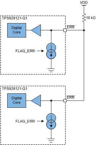
If multiple TPS929121-Q1 devices are used in one application, tying the ERR pins together achieves the one-fails-all-fail behavior in fail-safe states without master controlling. Any one of TPS929121-Q1 reports fault by pulling the ERR pin to low, and the low voltage on ERR bus is detected by other TPS929121-Q1 as Figure 8-9 illustrated. If the register EEP_OFAF is set to 1 for all TPS929121-Q1 devices having the ERR pins tied together, all TPS929121-Q1 devices turn off current for all output channels.
 Figure 8-9 ERR
Internal Block Diagram