JAJSKY0B June 2019 – July 2024 TPS99001-Q1
PRODUCTION DATA
- 1
- 1 特長
- 2 アプリケーション
- 3 概要
- 4 Pin Configuration and Functions
-
5 Specifications
- 5.1 Absolute Maximum Ratings
- 5.2 ESD Ratings
- 5.3 Recommended Operating Conditions
- 5.4 Thermal Information
- 5.5 Electrical Characteristics—Analog to Digital Converter
- 5.6 Electrical Characteristics—Voltage Regulators
- 5.7 Electrical Characteristics—Temperature and Voltage Monitors
- 5.8 Electrical Characteristics—Current Consumption
- 5.9 Power-Up Timing Requirements
- 5.10 Power-Down Timing Requirements
- 5.11 Timing Requirements—Sequencer Clock
- 5.12 Timing Requirements—Host and Diagnostic Port SPI Interface
- 5.13 Timing Requirements—ADC Interface
- 5.14 Switching Characteristics
-
6 Detailed Description
- 6.1 Overview
- 6.2 Functional Block Diagram
- 6.3 Feature Description
- 6.4 Device Functional Modes
- 6.5 Register Maps
- 7 Application and Implementation
- 8 Power Supply Recommendations
- 9 Layout
- 10Device and Documentation Support
- 11Revision History
- 12Mechanical, Packaging, and Orderable Information
パッケージ・オプション
メカニカル・データ(パッケージ|ピン)
- PZP|100
サーマルパッド・メカニカル・データ
- PZP|100
発注情報
9.1.4 Kelvin Sensing Connections
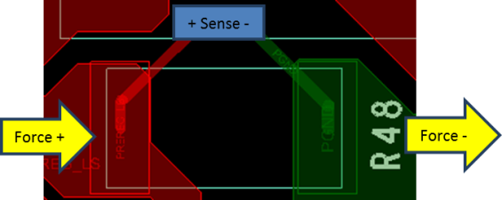
There are many places in the system design where the current through a signal path is measured by using a sense resistor in series with the signal path. In these cases, the resistor should be connected by using a “Kelvin” connection, or a “Force-Sense” connection. This means that two connections are made to the resistor that carry the high level of current, and two connections are made separately to measure the voltage across the resistor. This prevents the sense lines from being affected by the extra resistance of the copper traces, and makes the measurement more accurate. An example of the “Force-Sense” connection is shown in Figure 9-1.
 Figure 9-1 Kelvin Sensing Layout
The TPS99001-Q1 uses a sense resistor to measure the current delivered to the LEDs. These differential sense lines are the inputs to the part LS_SENSE_P and LS_SENSE_N. It is important to notice that although LS_SENSE_N may be electrically connected to ground by the netlist, this signal must be routed as a separate trace to prevent it from being affected by changes in the ground plane.