JAJSPB3 November   2022 TPSM82902

PRODUCTION DATA  

  1. 特長
  2. アプリケーション
  3. 概要
  4. Revision History
  5. Pin Configuration and Functions
  6. Specifications
    1. 6.1 Absolute Maximum Ratings
    2. 6.2 ESD Ratings
    3. 6.3 Recommended Operating Conditions
    4. 6.4 Thermal Information
    5. 6.5 Electrical Characteristics
    6. 6.6 Typical Characteristics
  7. Detailed Description
    1. 7.1 Overview
    2. 7.2 Functional Block Diagram
    3. 7.3 Feature Description
      1. 7.3.1 Mode Selection and Device Configuration (MODE/S-CONF)
      2. 7.3.2 Adjustable VO Operation (External Voltage Divider)
      3. 7.3.3 Setable VO Operation (VSET and Internal Voltage Divider)
      4. 7.3.4 Soft Start/Tracking (SS/TR)
      5. 7.3.5 Smart Enable with Precise Threshold
      6. 7.3.6 Power Good (PG)
      7. 7.3.7 Undervoltage Lockout (UVLO)
      8. 7.3.8 Current Limit And Short Circuit Protection
      9. 7.3.9 Thermal Shutdown
    4. 7.4 Device Functional Modes
      1. 7.4.1 Pulse Width Modulation (PWM) Operation
      2. 7.4.2 AEE (Automatic Efficiency Enhancement)
      3. 7.4.3 Power Save Mode Operation (Auto PFM/PWM)
      4. 7.4.4 100% Duty-Cycle Operation
      5. 7.4.5 Output Discharge Function
      6. 7.4.6 Starting into a Pre-Biased Load
  8. Application and Implementation
    1. 8.1 Application Information
    2. 8.2 Typical Application with Adjustable Output Voltage
      1. 8.2.1 Design Requirements
      2. 8.2.2 Detailed Design Procedure
        1. 8.2.2.1 Custom Design With WEBENCH® Tools
        2. 8.2.2.2 Programming the Output Voltage
        3. 8.2.2.3 Capacitor Selection
          1. 8.2.2.3.1 Output Capacitor
          2. 8.2.2.3.2 Input Capacitor
          3. 8.2.2.3.3 Soft-Start Capacitor
        4. 8.2.2.4 Tracking Function
      3. 8.2.3 Application Curves
    3. 8.3 Typical Application with Setable VO Using VSET
      1. 8.3.1 Design Requirements
      2. 8.3.2 Detailed Design Procedure
      3. 8.3.3 Application Curves
    4. 8.4 Power Supply Recommendations
    5. 8.5 Layout
      1. 8.5.1 Layout Guidelines
      2. 8.5.2 Layout Example
        1. 8.5.2.1 Thermal Considerations
  9. Device and Documentation Support
    1. 9.1 Device Support
      1. 9.1.1 Third-Party Products Disclaimer
      2. 9.1.2 Development Support
        1. 9.1.2.1 Custom Design With WEBENCH® Tools
    2. 9.2 Receiving Notification of Documentation Updates
    3. 9.3 サポート・リソース
    4. 9.4 Trademarks
    5. 9.5 Electrostatic Discharge Caution
    6. 9.6 Glossary
  10. 10Mechanical, Packaging, and Orderable Information

パッケージ・オプション

メカニカル・データ(パッケージ|ピン)
サーマルパッド・メカニカル・データ
発注情報
Soft-Start Capacitor

A capacitor connected between SS/TR pin and GND allows a user-programmable start-up slope of the output voltage.
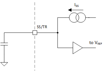
GUID-F9DB626F-84EF-477B-9BE1-BDE1B6AC71F8-low.gifFigure 8-2 Soft-Start Operation Simplified Schematic

An internal constant current source is provided to charge the external capacitance. The capacitor required for a given soft-start ramp time is given by:

Equation 11. GUID-1D471347-05D8-4463-8839-005ACB11EDFA-low.gif

where

  • CSS is the capacitance required at the SS/TR pin.
  • TSS is the desired soft-start ramp time.
  • ISS is the SS/TR source current, see the Electrical Characteristics.
  • VREF is the feedback regulation voltage divided by tracking gain (VFB/0.75), see the Electrical Characteristics.

The fastest achievable typical ramp time is 150 µs even if the external Css capacitance is lower than 680 pF or the pin is open.