JAJSO21B February 2022 – November 2022 TPSM82903
PRODUCTION DATA
- 1 特長
- 2 アプリケーション
- 3 概要
- 4 Revision History
- 5 Pin Configuration and Functions
- 6 Specifications
-
7 Detailed Description
- 7.1 Overview
- 7.2 Functional Block Diagram
- 7.3
Feature Description
- 7.3.1 Mode Selection and Device Configuration (MODE/S-CONF)
- 7.3.2 Adjustable VO Operation (External Voltage Divider)
- 7.3.3 Setable VO Operation (VSET and Internal Voltage Divider)
- 7.3.4 Soft Start/Tracking (SS/TR)
- 7.3.5 Smart Enable with Precise Threshold
- 7.3.6 Power Good (PG)
- 7.3.7 Undervoltage Lockout (UVLO)
- 7.3.8 Current Limit And Short Circuit Protection
- 7.3.9 Thermal Shutdown
- 7.4 Device Functional Modes
- 8 Application and Implementation
- 9 Device and Documentation Support
- 10Mechanical, Packaging, and Orderable Information
5 Pin Configuration and Functions

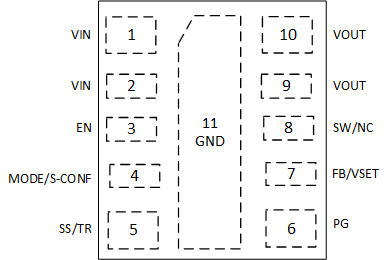
Figure 5-1 11-Pin SIS MicroSiP™ Package (Top View, Device Pins Face Down)
Table 5-1 Pin Functions
| Pin | I/O | Description | |
|---|---|---|---|
| Name | Number | ||
| VIN | 1, 2 | I | Power supply input pin. Ensure the input capacitor is connected as close as possible between the VIN and GND pins. |
| EN | 3 | I | Enable input pin. Connect to logic low to disable the device. Pull high to enable the device. Do not leave this pin unconnected. |
| MODE/ S-CONF | 4 | I | Device mode selection (auto PFM/PWM or forced PWM operation) and SmartConfig™ application. Connect high, low, or to a resistor to configure the device according to Table 7-2. Do not leave this pin unconnected. |
| SS/TR | 5 | I | Soft start/tracking pin. An external capacitor connected from this pin to GND defines the rise time for the internal reference voltage. The pin can also be used as an input for tracking and sequencing. The pin can be left floating for the fastest ramp-up time. |
| PG | 6 | O | Open-drain power-good output. High = VOUT is ready. Low = VOUT is below nominal regulation. This pin requires a pullup resistor. |
| FB/VSET | 7 | I | Depends on device configuration (see Section 7.3.1)
|
| SW/NC | 8 | NC | Switch pin of the converter. Do not connect, leave floating. |
| VOUT | 9, 10 | O | Output voltage pin. Connect directly to the positive pin of the output capacitor. |
| GND | 11 | — | Ground pin. It must be connected directly to the common ground plane. It must be soldered to achieve appropriate power dissipation and mechanical reliability. |