JAJSEK3B January 2018 – JANUARY 2019 TPSM846C24
PRODUCTION DATA.
- 1 特長
- 2 アプリケーション
- 3 概要
- 4 改訂履歴
- 5 Pin Configuration and Functions
- 6 Specifications
-
7 Detailed Description
- 7.1 Overview
- 7.2 Functional Block Diagram
- 7.3
Feature Description
- 7.3.1 Minimum Capacitance Requirements
- 7.3.2 Setting the Compensation Network
- 7.3.3 Transient Response
- 7.3.4 Setting the Output Voltage
- 7.3.5 Differential Remote Sense
- 7.3.6 Switching Frequency and Synchronization
- 7.3.7 Prebiased Output Start-Up
- 7.3.8 Power-Good (PGOOD) Indicator
- 7.3.9 Linear Regulators BP3 and BP6
- 7.3.10 Parallel Application
- 7.3.11 Parallel Operation
- 7.3.12 Overtemperature Protection
- 7.3.13 Overcurrent Protection
- 7.3.14 Output Overvoltage and Undervoltage Protection
- 7.4 Device Functional Modes
- 8 Application and Implementation
- 9 Power Supply Recommendations
- 10Layout
- 11デバイスおよびドキュメントのサポート
- 12メカニカル、パッケージ、および注文情報
10.5 Mounting and Thermal Profile Recommendation
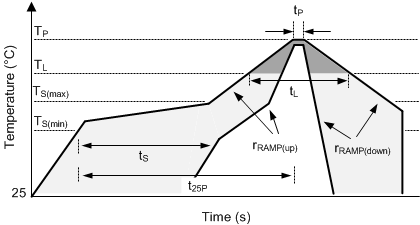
Proper mounting technique adequately covers the exposed thermal pad with solder. Excessive heat during the reflow process can affect electrical performance. Figure 26 shows the recommended reflow-oven thermal profile. Proper post-assembly cleaning is also critical to device performance. Refer to Power Module MSL Ratings and Reflow Ratings for more information.
 Figure 26. Recommended Reflow-Oven Thermal Profile
 Table 5. Recommended Thermal Profile Parameters
| PARAMETER | MIN | TYP | MAX | UNIT | |
|---|---|---|---|---|---|
| RAMP UP AND RAMP DOWN | |||||
| rRAMP(up) | Average ramp-up rate, TS(max) to TP | 3 | °C/s | ||
| rRAMP(down) | Average ramp-down rate, TP to TS(max) | 6 | °C/s | ||
| PRE-HEAT | |||||
| TS | Preheat temperature | 150 | 200 | °C | |
| tS | Preheat time, TS(min) to TS(max) | 60 | 120 | s | |
| REFLOW | |||||
| TL | Liquidous temperature | 217 | °C | ||
| TP | Peak temperature | 260 | °C | ||
| tL | Time maintained above liquidous temperature, TL | 60 | 150 | s | |
| tP | Time maintained within 5°C of peak temperature, TP | 20 | 30 | s | |
| t25P | Total time from 25°C to peak temperature, TP | 480 | s | ||