at TA = 25°C, temperature curves
specify ambient temperature, VDD = 3.3V, 50Ω single-ended input, and 100Ω
differential output (unless otherwise noted)
 Figure 5-1 Power
Gain Across Temperature
 Figure 5-3 Return Loss Across
Temperature
 Figure 5-5 Reverse Isolation Across
Temperature
| PO /tone = –4dBm, 10MHz tone
spacing |
Figure 5-7 OIP3 Across
Temperature
At
(2f1-f2) frequency,
f1 < f2; PO
/tone = –4dBm,
10MHz tone
spacing |
Figure 5-9 IMD3 Lower Across
Temperature
At
(2f2-f1) frequency,
f1 < f2; PO
/tone = –4dBm,
10MHz tone
spacing |
Figure 5-11 IMD3 Higher Across
Temperature
At
(f2-f1) frequency,
f2 > f1; PO
/tone = –4dBm,
10MHz tone
spacing |
Figure 5-13 OIP2 Lower Across
Temperature
At
(f2+f1) frequency,
f2 > f1; PO
/tone = –4dBm,
10MHz tone
spacing |
Figure 5-15 OIP2 Higher Across
Temperature
At
(f2-f1) frequency,
f2 > f1; PO
/tone = –4dBm,
10MHz tone
spacing |
Figure 5-17 IMD2 Lower Across
Temperature
At
(f2+f1) frequency,
f2 > f1; PO
/tone = –4dBm,
10MHz tone
spacing |
Figure 5-19 IMD2 Higher Across
Temperature Figure 5-21 HD2 Across
Temperature
 Figure 5-23 HD3 Across
Temperature
 Figure 5-25 HD2 vs Output
Power
 Figure 5-27 Output P1dB Across
Temperature
 Figure 5-29 NF Across
Temperature
 Figure 5-31 Gain Imbalance
 Figure 5-33 CMRR Across
Temperature
| Input = –2dBm, f = 500MHz |
Figure 5-35 Overdrive Recovery
| Low
frequency cut-off as a function of ac-coupling
cap |
Figure 5-37 Low Frequency Gain
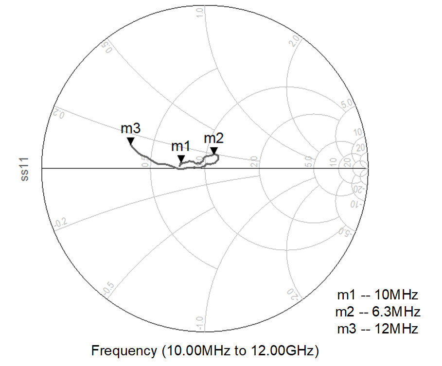
Response Figure 5-39 Single-Ended S11
 Figure 5-2 Power
Gain Across VDD
 Figure 5-4 Return Loss Across
VDD
 Figure 5-6 Reverse Isolation Across
VDD
| PO /tone = –4dBm, 10MHz tone
spacing |
Figure 5-8 OIP3 Across
VDD
At
(2f1-f2) frequency,
f1 < f2; PO
/tone = –4dBm,
10MHz tone
spacing |
Figure 5-10 IMD3 Lower Across
VDD
At
(2f2-f1) frequency,
f1 < f2; PO
/tone = –4dBm,
10MHz tone
spacing |
Figure 5-12 IMD3 Higher Across
VDD
At
(f2-f1) frequency,
f2 > f1; PO
/tone = –4dBm,
10MHz tone
spacing |
Figure 5-14 OIP2 Lower Across
VDD
At
(f2+f1) frequency,
f2 > f1; PO
/tone = –4dBm,
10MHz tone
spacing |
Figure 5-16 OIP2 Higher Across
VDD
At
(f2-f1) frequency,
f2 > f1; PO
/tone = –4dBm,
10MHz tone
spacing |
Figure 5-18 IMD2 Lower Across
VDD
At
(f2+f1) frequency,
f2 > f1; PO
/tone = –4dBm,
10MHz tone
spacing |
Figure 5-20 IMD2 Higher Across
VDD Figure 5-22 HD2 Across
VDD
 Figure 5-24 HD3 Across
VDD
 Figure 5-26 HD3 vs Output
Power
 Figure 5-28 Output P1dB Across
VDD
 Figure 5-30 NF Across
VDD
 Figure 5-32 Phase Imbalance
 Figure 5-34 CMRR Across
VDD
 Figure 5-36 Saturation Voltage
(Differential)
 Figure 5-38 Additive (Residual) Phase
Noise
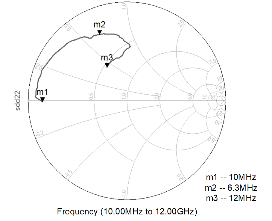
 Figure 5-40 Differential S22


 Figure 5-39 Single-Ended S11


 Figure 5-40 Differential S22