at TA = 25℃, VS+
= 5 V, VS– = 0 V, floating VOCM, PDx, and MODE pins, VICM =
midsupply, D2D ac-coupled input/output configuration with ZS = 100 Ω,
ZL = 100 Ω, external input resistor network (see Figure 8-3), ambient temperatures shown, and resistor network included as part of DUT
characteristic plots (unless otherwise noted)

| PIN = –20 dBm at each input pin with
50-Ω source |
Figure 6-1 Power Gain (S21) Across
Temperature
| PIN = –20 dBm at each input pin with
50-Ω source |
Figure 6-3 Input Return Loss (S11)
Across Temperature
| PIN = –20 dBm at each input pin with
50-Ω source |
Figure 6-5 Output Return Loss (S22)
Across Temperature
| PO/tone = –5 dBm, 2‑MHz tone
spacing |
Figure 6-7 OIP3 Across Temperature
| PO/tone = 1 dBm,
2‑MHz tone spacing |
Figure 6-9 OIP3 Across Temperature
At
(2f1–f2) frequency where
f1 < f2,
PO/tone = –5
dBm, 2‑MHz tone spacing |
Figure 6-11 IMD3 Lower Across
Temperature
At
(2f2–f1) frequency where
f1 < f2,
PO/tone = –5
dBm, 2‑MHz tone spacing |
Figure 6-13 IMD3 Higher Across Temperature
PO/tone = 1 dBm, 2‑MHz tone
spacing,
dc-coupled
inputs with VICM forced through bias
tees |
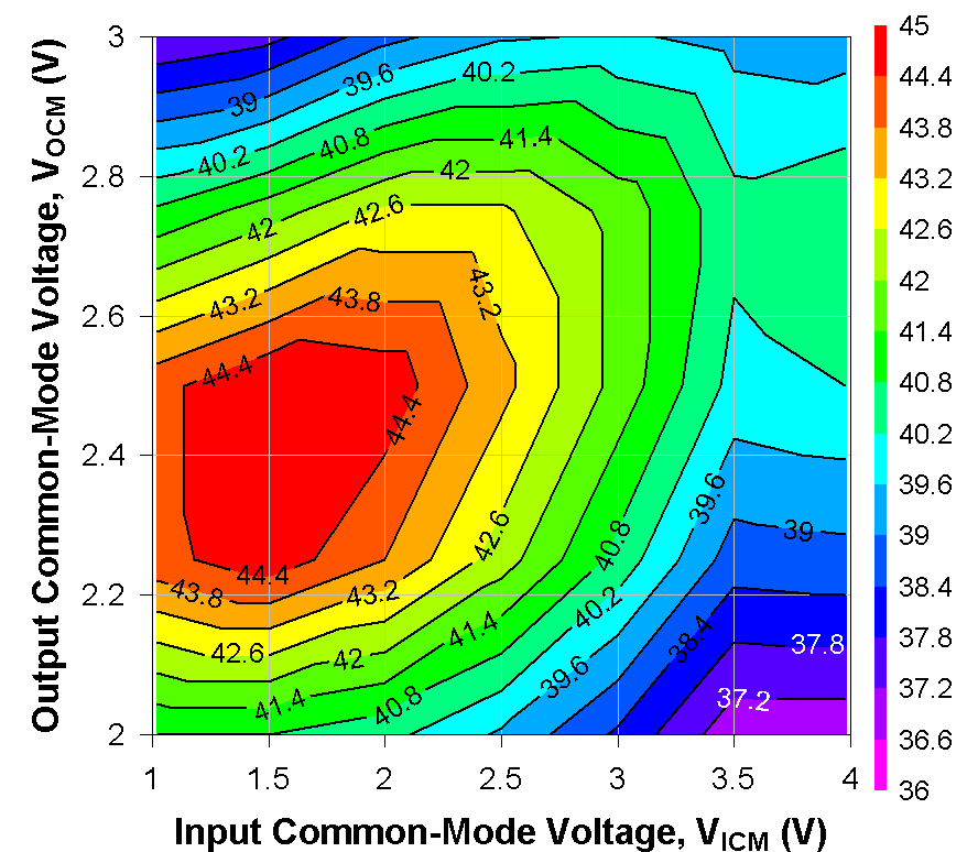
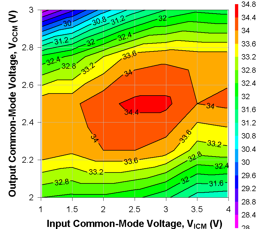
Figure 6-15 OIP3 Across
VICM and VOCM at 500 MHz
PO/tone = 1 dBm, 2‑MHz tone
spacing,
dc-coupled
inputs with VICM forced through bias
tees |
Figure 6-17 OIP3 Across VICM and VOCM at 4 GHz Figure 6-19 OP1dB Across Temperature
 Figure 6-21 Noise Figure Across Temperature
| Channel 1, PIN
at each input pin with 50-Ω source |
Figure 6-23 Power Gain (S21) Across Input Power Levels
| S2D, PIN = –20
dBm at each input pin with 50-Ω source |
Figure 6-25 S-Parameters in S2D
Configuration
| S2D configuration,
PO/tone = 1 dBm, 2‑MHz tone
spacing |
Figure 6-27 OIP3 Across Supply
Voltage
| S2D, PIN = –20
dBm at each input pin with 50-Ω source |
Figure 6-29 CMRR in S2D
Configuration
| S2D configuration,
VS+ = 2.5 V, VS– = –2.5
V |
Figure 6-31 Step Response
Voltage gain
(AV) ≈ 1.5 V/V,
VOZYx = Y × VOP1x, where Z =
P or M and Y = 2 or 5 |
Figure 6-33 Overload Recovery Response
and Timing
| PIN = –20 dBm at each input pin with
50-Ω source |
Figure 6-2 Power Gain (S21) Across
Supply Voltage
| PIN = –20 dBm at each input
pin with 50-Ω source |
Figure 6-4 Input Return Loss (S11)
Across Supply Voltage
| PIN = –20 dBm at each input pin with
50-Ω source |
Figure 6-6 Reverse Isolation (S12)
Across Temperature
| PO/tone = –5
dBm, 2‑MHz tone spacing |
Figure 6-8 OIP3 Across Supply Voltage
| PO/tone = 1 dBm,
2‑MHz tone spacing |
Figure 6-10 OIP3 Across Supply Voltage
At
(2f1–f2) frequency where
f1 < f2,
PO/tone = –5
dBm, 2‑MHz tone spacing |
Figure 6-12 IMD3 Lower Across Supply Voltage
At
(2f2–f1) frequency where
f1 < f2,
PO/tone = –5
dBm, 2‑MHz tone spacing |
Figure 6-14 IMD3 Higher Across Supply Voltage
PO/tone = 1 dBm, 2‑MHz tone
spacing,
dc-coupled
inputs with VICM forced through bias
tees |
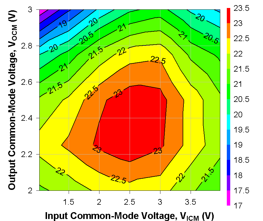
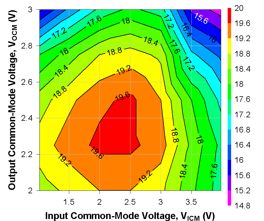
Figure 6-16 OIP3 Across
VICM and VOCM at 2 GHz
PO/tone = 1 dBm, 2‑MHz tone
spacing,
dc-coupled
inputs with VICM forced through bias
tees |
Figure 6-18 OIP3 Across VICM and VOCM at 5 GHz Figure 6-20 OP1dB Across Supply Voltage
 Figure 6-22 Noise Figure Across Supply Voltage
| Channel 1, D2D
configuration |
Figure 6-24 Input Power vs. Output
Power
| S2D, PO/tone =
–5 dBm, 2‑MHz tone spacing |
Figure 6-26 OIP3 Across Supply Voltage
in S2D Configuration Figure 6-28 OP1dB Across Supply
Voltage
| S2D, PIN = –20
dBm at each input pin with 50-Ω source |
Figure 6-30 Gain and Phase Imbalance
in S2D Configuration
| PIN = –20 dBm at
each input pin with 50-Ω source |
Figure 6-32 Channel-to-Channel
Isolation Figure 6-34 Power Up and Power Down
Timing


