JAJSKD0
December 2023
TRF1305B2
PRODUCTION DATA
1
1
特長
2
アプリケーション
3
概要
4
Device Comparison
5
Pin Configuration and Functions
6
Specifications
6.1
Absolute Maximum Ratings
6.2
ESD Ratings
6.3
Recommended Operating Conditions
6.4
Thermal Information
6.5
Electrical Characteristics - TRF1305B2
6.6
Typical Characteristics - TRF1305B2
7
Detailed Description
7.1
Overview
7.2
Functional Block Diagram
7.3
Feature Description
7.3.1
Fully Differential Amplifier
7.3.2
Output Common-Mode Control
7.3.3
Internal Resistor Configuration
7.4
Device Functional Modes
7.4.1
MODE Pin
7.4.1.1
Input Common-Mode Extension
7.4.2
Power-Down Mode
8
Application and Implementation
8.1
Application Information
8.1.1
Input and Output Interface Considerations
8.1.1.1
Single-Ended Input
8.1.1.2
Differential Input
8.1.1.3
DC Coupling Considerations
8.1.2
Gain Adjustment With External Resistors in a Differential Input Configuration
8.2
Typical Application
8.2.1
TRF1305x2 as ADC Driver in a Zero-IF Receiver
8.2.1.1
Design Requirements
8.2.1.2
Detailed Design Procedure
8.2.1.3
Application Curves
8.3
Power Supply Recommendations
8.3.1
Supply Voltages
8.3.2
Single-Supply Operation
8.3.3
Split-Supply Operation
8.3.4
Supply Decoupling
8.4
Layout
8.4.1
Layout Guidelines
8.4.1.1
Thermal Considerations
8.4.2
Layout Example
9
Device and Documentation Support
9.1
ドキュメントの更新通知を受け取る方法
9.2
サポート・リソース
9.3
Trademarks
9.4
静電気放電に関する注意事項
9.5
用語集
10
Revision History
11
Mechanical, Packaging, and Orderable Information
パッケージ・オプション
メカニカル・データ(パッケージ|ピン)
RYP|16
MPQF635C
サーマルパッド・メカニカル・データ
発注情報
jajskd0_oa
8.2.1.3
Application Curves
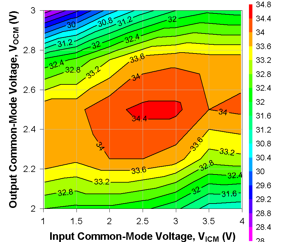
f = 2 GHz, P
O
/tone = 1 dBm, 2‑MHz tone spacing
Figure 8-8
OIP3 Across Input and Output Common-Mode Voltage
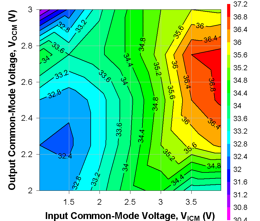
f = 2 GHz, P
O
/tone = –5 dBm, 2‑MHz tone spacing
Figure 8-9
OIP3 Across Input and Output Common-Mode Voltage