SLWS181K October 2005 – December 2015 TRF3761-A , TRF3761-B , TRF3761-C , TRF3761-E , TRF3761-F , TRF3761-G , TRF3761-H , TRF3761-J
PRODUCTION DATA.
- 1 Features
- 2 Applications
- 3 Description
- 4 Revision History
- 5 Device Comparison Table
- 6 Pin Configuration and Functions
-
7 Specifications
- 7.1 Absolute Maximum Ratings
- 7.2 Recommended Operating Conditions
- 7.3 Thermal Information
- 7.4 Electrical Characteristics
- 7.5 Electrical Characteristics, TRF3761-A
- 7.6 Electrical Characteristics,TRF3761-B
- 7.7 Electrical Characteristics, TRF3761-C
- 7.8 Electrical Characteristics, TRF3761-D
- 7.9 Electrical Characteristics, TRF3761-E
- 7.10 Electrical Characteristics, TRF3761-F
- 7.11 Electrical Characteristics, TRF3761-G
- 7.12 Electrical Characteristics, TRF3761-H
- 7.13 Electrical Characteristics, TRF3761-J
- 7.14 Timing Requirements
- 7.15
Typical Characteristics
- 7.15.1 Typical Characteristics, TRF3761-A (See )
- 7.15.2 Typical Characteristics, TRF3761-B (See )
- 7.15.3 Typical Characteristics, TRF3761-C (See )
- 7.15.4 Typical Characteristics, TRF3761-D (See )
- 7.15.5 Typical Characteristics, TRF3761-E (See )
- 7.15.6 Typical Characteristics, TRF3761-F (See )
- 7.15.7 Typical Characteristics, TRF3761-G (See )
- 7.15.8 Typical Characteristics, TRF3761-H (See )
- 7.15.9 Typical Characteristics, TRF3761-J (See )
-
8 Detailed Description
- 8.1 Overview
- 8.2 Functional Block Diagram
- 8.3 Feature Description
- 8.4 Device Functional Modes
- 8.5 Programming
- 8.6 Register Maps
- 9 Application and Implementation
- 10Power Supply Recommendations
- 11Layout
- 12Device and Documentation Support
- 13Mechanical, Packaging, and Orderable Information
パッケージ・オプション
メカニカル・データ(パッケージ|ピン)
- RHA|40
サーマルパッド・メカニカル・データ
- RHA|40
発注情報
11 Layout
11.1 Layout Guidelines
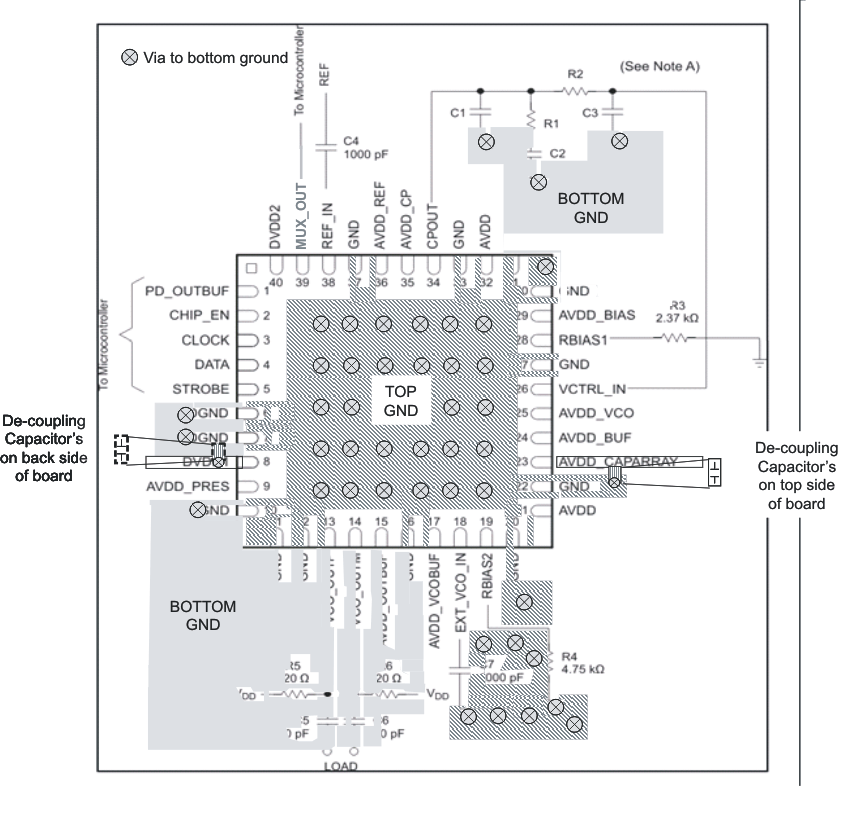
When designing the complete PLL, this section is of paramount importance in achieving the desired performance. Wherever possible, a multi-layer PCB board should be used, with at least one dedicated ground plane. A dedicated power plane (split between the supplies if necessary) is also recommended. The impedance of all RF traces (the VCO output and feedback into the PLL) should be controlled to 50Ω. All small value (10pF and 0.1µF) decoupling capacitors should be placed as close to the device pins as possible. It is also recommended that both top and bottom layers of the circuit board be flooded with ground, with plenty of ground vias dispersed as appropriate. Because the digital lines are not in use during normal operation of the device and are only used to program the device on start up and during frequency changes the analog grounds (GND) and digital grounds (DGND) are tied to the same ground plane. The most sensitive part of any PLL is the section between the charge pump output and the input to the VCO. This includes the loop filter components, and the corresponding traces. The charge pump is a precision element of the PLL and any extra leakage on its path can adversely affect performance. Extra care should be given to ensure that parasitics are minimized in the charge pump output, and that the trace runs are short and optimized. Similarly, it is also recommend that extra care is taken in ensuring that any flux residue is thoroughly cleaned and moisture baked out of the PCB. From an EMI perspective, and since the synthesizer is typically a small portion of a bigger, complex circuit board, shielding is recommended to minimize EMI effects.
