TRF37x32 Dual Down Converter Mixer With Integrated IF AMP
1 Features
- Device Family Supports Wide RF Input Range
- TRF37A32: 400 - 1700 MHz
- TRF37B32: 700 - 2700 MHz
- TRF37C32: 1700 - 3800 MHz
- Gain: 10 dB
- Noise Figure: 9.5 dB
- Input IP3: 30 dBm
- 500 mW per Channel Power Dissipation
- Single Ended RF Input
- IF Frequency Range from 30 MHz to 600 MHz
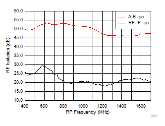
- 45 dB Isolation between Channels
- Low Power Mode Option
- Independent Power Down Control
- Single 3.3V Supply
- No External Matching Required
2 Applications
- Wireless Infrastructure
- WCDMA, TD-SCDMA
- LTE, TD-LTE
- Multicarrier GSM (MC-GSM)
- Point-to-Point Microwave
- Software Defined Radios (SDR)
- Radar Receiver
- Satellite Communications
3 Description
The TRF37x32 is a wideband dual down converter mixer with integrated IF amplifier. The device employs integrated baluns for single ended RF and LO inputs. The IF amplifier operates from 30 MHz to 600 MHz in an open collector topology to support a variety of IF frequencies and bandwidths. The TRF37x32 provides excellent mixer linearity and noise performance and offers good isolation between channels for operation with diversity applications. The device operates with low power dissipation and further provides an option for a low power mode for power sensitive applications. Each channel can be independently powered down with fast response times to allow operation in time domain duplexed (TDD) applications.
Device Information(1)
| PART NUMBER | PACKAGE | BODY SIZE (NOM) |
|---|---|---|
| TRF37A32 | WQFN (32) | 5.00mm x 5.00mm |
| TRF37B32 | ||
| TRF37C32 |
- For all available packages, see the orderable addendum at the end of the datasheet.
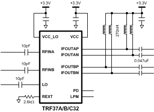
4 Simplified Schematic
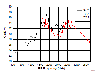
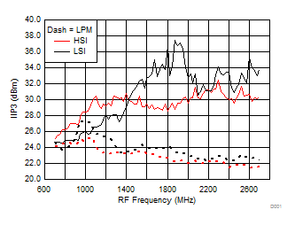
IIP3 Performance Across Frequency
5 Revision History
Changes from * Revision (May 2014) to A Revision
- Added Typical Characteristics, Feature Description section, Device Functional Modes, Application and Implementation section, Power Supply Recommendations section, and Layout sectionGo
- Replaced the Handling Ratings table with the ESD Ratings tableGo
6 Pin Configuration and Functions
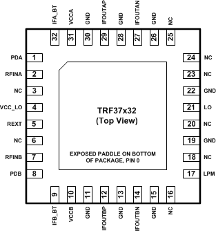
Pin Functions
| PIN | I/O | DESCRIPTION | |
|---|---|---|---|
| NAME | NO. | ||
| PDA | 1 | Digital Input | Power down for channel A (1 = PD; 0 or open = powered) |
| RFINA | 2 | Analog Input | RF input for channel A |
| NC | 3 | N/A | No connect |
| VCC_LO | 4 | Supply | VCC supply for the LO circuitry |
| REXT | 5 | Bias | External bias resistor |
| NC | 6 | N/A | No connect |
| RFINB | 7 | Analog Input | RF input for channel B |
| PDB | 8 | Digital Input | Power down for channel B (1 = PD; 0 or open = powered) |
| IFB_BT | 9 | N/A | IF channel B bias control; leave unconnected |
| VCCB | 10 | Supply | Power supply for channel B |
| GND | 11 | Ground | Ground |
| IFOUTBP | 12 | Analog Output | IF out channel B: positive |
| GND | 13 | Ground | Ground |
| IFOUTBN | 14 | Analog Output | IF out channel B: negative |
| GND | 15 | Ground | Ground |
| NC | 16 | N/A | No connect |
| LPM | 17 | Digital Input | Low power mode (0 = normal; 1 = low power) |
| NC | 18 | N/A | No connect |
| GND | 19 | Ground | Ground |
| NC | 20 | N/A | No connect |
| LO | 21 | Analog Input | Local oscillator (LO) input |
| GND | 22 | Ground | Ground |
| NC | 23 | N/A | No connect |
| NC | 24 | N/A | No connect |
| NC | 25 | N/A | No connect |
| GND | 26 | Ground | Ground |
| IFOUTAN | 27 | Analog Output | IF out channel A: negative |
| GND | 28 | Ground | Ground |
| IFOUTAP | 29 | Analog Output | IF out channel A: positive |
| GND | 30 | Ground | Ground |
| VCCA | 31 | Supply | Power supply for channel A |
| IFA_BT | 32 | N/A | IF channel A bias control; leave unconnected |
7 Specifications
7.1 Absolute Maximum Ratings
over operating free-air temperature range (unless otherwise noted) (1)| MIN | MAX | UNIT | ||
|---|---|---|---|---|
| Input voltage | –0.3 | 3.6 | V | |
| Storage temperature, TSTG | –40 | 150 | °C |
7.2 ESD Ratings
| VALUE | UNIT | ||||
|---|---|---|---|---|---|
| V(ESD) | Electrostatic discharge | Human-body model (HBM), per ANSI/ESDA/JEDEC JS-001(1) | All pins except XIFOUTAP, IFOUTAN, IFOUTBP, and IFOUTBN | ±2500 | V |
| Pins XIFOUTAP, IFOUTAN, IFOUTBP, and IFOUTBN (2) | ±100 | ||||
| Charged-device model (CDM), per JEDEC specification JESD22-C101(3) | ±1000 | ||||
7.3 Recommended Operating Conditions
over operating free-air temperature range (unless otherwise noted)| MIN | NOM | MAX | UNIT | ||
|---|---|---|---|---|---|
| Operating virtual junction temperature range, TJ | –40 | 125 | °C | ||
7.4 Thermal Information
| THERMAL METRIC(1) | RTV | UNIT | |
|---|---|---|---|
| 32 PINS | |||
| RθJA | Junction-to-ambient thermal resistance | 32.3 | °C/W |
| RθJCtop | Junction-to-case (top) thermal resistance | 19.8 | |
| RθJB | Junction-to-board thermal resistance | 5.9 | |
| ψJT | Junction-to-top characterization parameter | 0.2 | |
| ψJB | Junction-to-board characterization parameter | 5.9 | |
| RθJCbot | Junction-to-case (bottom) thermal resistance | 1.3 | |
7.5 Electrical Characteristics, TRF37A32
TA = 25°C, VCC = 3.3 V; PRF = –10 dBm; PLO = 0 dBm; FIF = 200 MHz; Low Side Injection, LPM = 0 (unless otherwise noted)| PARAMETER | TEST CONDITIONS | MIN | TYP | MAX | UNIT | |
|---|---|---|---|---|---|---|
| DC Parameters | ||||||
| VCC | Supply Voltage | 3.15 | 3.3 | 3.45 | V | |
| ICC | Supply Current | FLO = 750 MHz | 280 | mA | ||
| Pdiss | Total Power Dissipation | FLO = 750 MHz | 0.92 | W | ||
| Power Down Current | 2 | mA | ||||
| RF Frequency Range | ||||||
| FRF | Frequency Range | 400 | 1700 | MHz | ||
| RF Specifications | ||||||
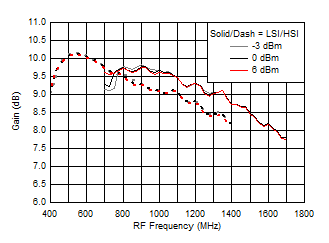
| G | Gain | FRF = 950 MHz (LSI) | 9.6 | dB | ||
| Gvar | Gain Variation over Frequency | within any 200 MHz Band | 0.5 | dB | ||
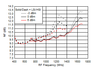
| NF | SSB Noise Figure | FRF = 950 MHz (LSI) | 9.6 | dB | ||
| SSB Noise Figure with Blocker | 5 dBm blocker signal Δf > 50 MHz |
17 | dB | |||
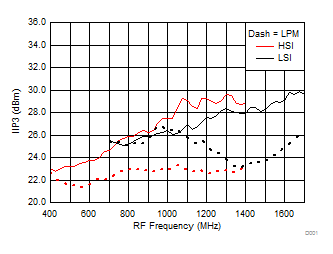
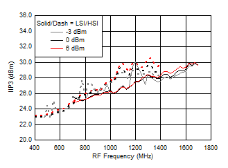
| IIP3 | Input 3rd Order Intercept Point | FRF = 950 MHz (LSI), Fspacing = 20 MHz |
26 | dBm | ||
| OIP3 | Output 3rd Order Intercept Point | FRF = 950 MHz (LSI), Fspacing = 20 MHz |
35.6 | dBm | ||
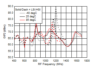
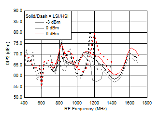
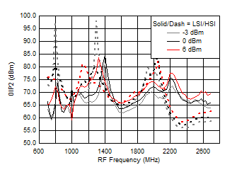
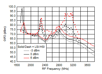
| OIP2 | Output 2nd Order Intercept Point | FRF = 950 MHz (LSI) | 65 | dBm | ||
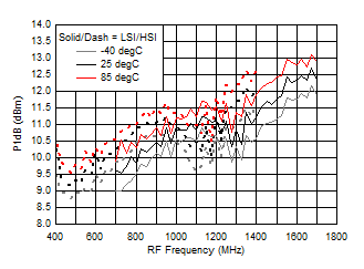
| IP1dB | Input 1 dB Compression Point | FRF = 950 MHz (LSI) | 11 | dBm | ||
| ZIN | Input Impedance | 50 | Ω | |||
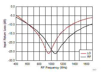
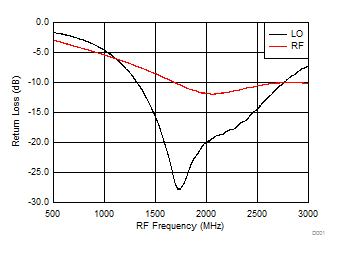
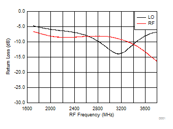
| RLi | Input Return Loss | FRF = 800 - 1400 MHz (LSI) | 15 | dB | ||
| LO Input | ||||||
| PLO | LO Drive Level | –3 | 0 | 6 | dBm | |
| FLO | LO Frequency Range | 600 | 1400 | MHz | ||
| ZIN | Input Impedance | 50 | Ω | |||
| RLi | Input Return Loss | FRF = 750 - 1150 MHz | 15 | dB | ||
| Low Power Mode: LPM = 1 | ||||||
| ICC | Supply Current | FLO = 750 MHz | 200 | mA | ||
| Pdiss | Total Power Dissipation | FLO = 750 MHz | 0.66 | W | ||
| G | Gain | FRF = 950 MHz (LSI) | 9.2 | dB | ||
| NF | SSB Noise Figure | FRF = 950 MHz (LSI) | 9.6 | dB | ||
| IIP3 | Input 3rd Order Intercept Point | FRF = 950 MHz (LSI), Fspacing = 20 MHz |
26 | dBm | ||
| IP1dB | Input 1 dB Compression Point | FRF = 950 MHz (LSI) | 11 | dBm | ||
| Isolation | ||||||
| Channel Isolation | Drive RFinA/B IFoutA/B-IFoutB/A FRF = 950 MHz |
50 | dB | |||
| RF to IF Isolation | FRF = 950 MHz | 20 | dB | |||
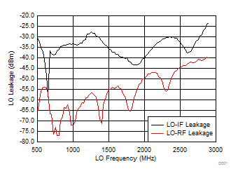
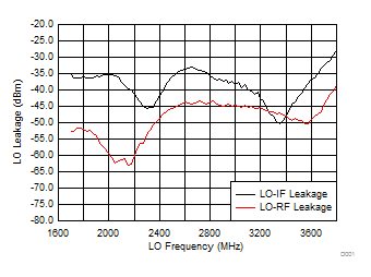
| LO to RF Leakage | PLO = 0 dBm | –55 | dBm | |||
| LO to IF Leakage | PLO = 0 dBm | –45 | dBm | |||
| Spurious | ||||||
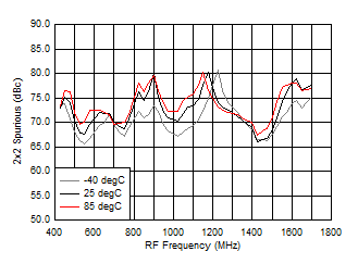
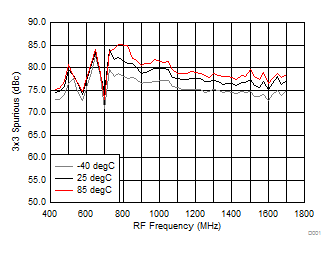
| 2x2 Spurious Product | 2RF - 2LO | 65 | dBc | |||
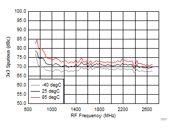
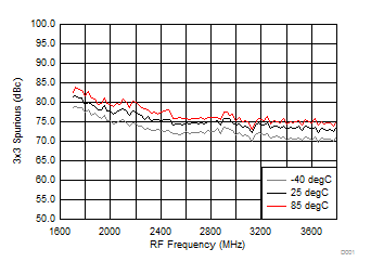
| 3x3 Spurious Product | 3RF - 3LO | 70 | dBc | |||
| IF Output | ||||||
| ZL | Differential Output Impedance Load | 200 | Ω | |||
| FIF | Frequency Range | 1 dB corner frequency | 30 | 600 | MHz | |
| DC Bias Range | Externally supplied DC bias through RF choke | 3.3 | V | |||
7.6 Electrical Characteristics, TRF37B32
TA = 25°C, VCC = 3.3 V; PRF = –10 dBm; PLO = 0 dBm; FIF = 200 MHz; Low Side Injection, LPM = 0 (unless otherwise noted)| PARAMETER | TEST CONDITIONS | MIN | TYP | MAX | UNIT | |
|---|---|---|---|---|---|---|
| DC Parameters | ||||||
| VCC | Supply Voltage | 3.15 | 3.3 | 3.45 | V | |
| ICC | Supply Current | FLO = 1750 MHz | 305 | mA | ||
| Pdiss | Total Power Dissipation | FLO = 1750 MHz | 1 | W | ||
| Power Down Current | 2 | mA | ||||
| RF Frequency Range | ||||||
| FRF | Frequency Range | 700 | 2700 | MHz | ||
| RF Specifications | ||||||
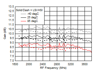
| G | Gain | FRF = 1950 MHz (LSI) | 10 | dB | ||
| Gvar | Gain Variation over Frequency | within any 200 MHz Band | 0.5 | dB | ||
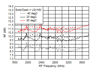
| NF | SSB Noise Figure | FRF = 1950 MHz (LSI) | 9.2 | dB | ||
| SSB Noise Figure with Blocker | 5 dBm blocker signal Δf > 50 MHz |
15.5 | dB | |||
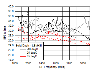
| IIP3 | Input 3rd Order Intercept Point | FRF = 1950 MHz (LSI), Fspacing = 20 MHz |
32 | dBm | ||
| OIP3 | Output 3rd Order Intercept Point | FRF = 1950 MHz (LSI), Fspacing = 20 MHz |
42 | dBm | ||
| OIP2 | Output 2nd Order Intercept Point | FRF = 1950 MHz (LSI) | 70 | dBm | ||
| IP1dB | Input 1 dB Compression Point | FRF = 1950 MHz (LSI) | 10.8 | dBm | ||
| ZIN | Input Impedance | 50 | Ω | |||
| RLi | Input Return Loss | FRF = 1700 - 2700 MHz (LSI) | 10 | dB | ||
| LO Input | ||||||
| PLO | LO Drive Level | –3 | 0 | 6 | dBm | |
| FLO | LO Frequency Range | 500 | 2900 | MHz | ||
| ZIN | Input Impedance | 50 | Ω | |||
| RLi | Input Return Loss | FRF = 1500 - 2450 MHz | 15 | dB | ||
| Low Power Mode: LPM = 1 | ||||||
| ICC | Supply Current | FLO = 1750 MHz | 220 | mA | ||
| Pdiss | Total Power Dissipation | FLO = 1750 MHz | 0.73 | W | ||
| G | Gain | FRF = 1950 MHz (LSI) | 9.2 | dB | ||
| NF | SSB Noise Figure | FRF = 1950 MHz (LSI) | 9.2 | dB | ||
| IIP3 | Input 3rd Order Intercept Point | FRF = 1950 MHz (LSI), Fspacing = 20 MHz |
23 | dBm | ||
| IP1dB | Input 1 dB Compression Point | FRF = 1950 MHz (LSI) | 10.7 | dBm | ||
| Isolation | ||||||
| Channel Isolation | Drive RFinA/B IFoutA/B-IFoutB/A FRF = 1950 MHz |
45 | dB | |||
| RF to IF Isolation | FRF = 1950 MHz | 22 | dB | |||
| LO to RF Leakage | PLO = 0 dBm | –50 | dBm | |||
| LO to IF Leakage | PLO = 0 dBm | –42 | dBm | |||
| Spurious | ||||||
| 2x2 Spurious Product | 2RF - 2LO | 70 | dBc | |||
| 3x3 Spurious Product | 3RF - 3LO | 75 | dBc | |||
| IF Output | ||||||
| ZL | Differential Output Impedance Load | 200 | Ω | |||
| FIF | Frequency Range | 1 dB corner frequency | 30 | 600 | MHz | |
| DC Bias Range | Externally supplied DC bias through RF choke | 3.3 | V | |||
7.7 Electrical Characteristics, TRF37C32
TA = 25°C, VCC = 3.3 V; PRF = –10 dBm; PLO = 0 dBm; FIF = 200 MHz; Low Side Injection, LPM = 0 (unless otherwise noted)| PARAMETER | TEST CONDITIONS | MIN | TYP | MAX | UNIT | |
|---|---|---|---|---|---|---|
| DC Parameters | ||||||
| VCC | Supply Voltage | 3.15 | 3.3 | 3.45 | V | |
| ICC | Supply Current | FLO = 2300 MHz | 325 | mA | ||
| Pdiss | Total Power Dissipation | FLO = 2300 MHz | 1.1 | W | ||
| Power Down Current | 2 | mA | ||||
| RF Frequency Range | ||||||
| FRF | Frequency Range | 1700 | 3800 | MHz | ||
| RF Specifications | ||||||
| G | Gain | FRF = 2500 MHz (LSI) | 9.8 | dB | ||
| Gvar | Gain Variation over Frequency | within any 200 MHz Band | 0.5 | dB | ||
| NF | SSB Noise Figure | FRF = 2500 MHz (LSI) | 9.9 | dB | ||
| SSB Noise Figure with Blocker | 5 dBm blocker signal Δf > 50 MHz |
17.5 | dB | |||
| IIP3 | Input 3rd Order Intercept Point | FRF = 2500 MHz (LSI) Fspacing = 20 MHz |
29 | dBm | ||
| OIP3 | Output 3rd Order Intercept Point | FRF = 2500 MHz (LSI) Fspacing = 20 MHz |
38.8 | dBm | ||
| OIP2 | Output 2nd Order Intercept Point | FRF = 2500 MHz (LSI) | 65 | dBm | ||
| IP1dB | Input 1 dB Compression Point | FRF = 2500 MHz (LSI) | 11.5 | dBm | ||
| ZIN | Input Impedance | 50 | Ω | |||
| RLi | Input Return Loss | 8 | dB | |||
| LO Input | ||||||
| PLO | LO Drive Level | –3 | 0 | 6 | dBm | |
| FLO | LO Frequency Range | 1500 | 3600 | MHz | ||
| ZIN | Input Impedance | 50 | Ω | |||
| RLi | Input Return Loss | FRF = 2800 - 3400 MHz | 10 | dB | ||
| Low Power Mode: LPM = 1 | ||||||
| ICC | Supply Current | FLO = 2300 MHz | 230 | mA | ||
| Pdiss | Total Power Dissipation | FLO = 2300 MHz | 0.76 | W | ||
| G | Gain | FRF = 2500 MHz (LSI) | 9.2 | dB | ||
| NF | SSB Noise Figure | FRF = 2500 MHz (LSI) | 9.9 | dB | ||
| IIP3 | Input 3rd Order Intercept Point | FRF = 2500 MHz (LSI), Fspacing = 20 MHz |
22 | dBm | ||
| IP1dB | Input 1 dB Compression Point | FRF = 2500 MHz (LSI) | 11.5 | dBm | ||
| Isolation | ||||||
| Channel Isolation | Drive RFinA/B IFoutA/B-IFoutB/A FRF = 2500 MHz |
48 | dB | |||
| RF to IF Isolation | FRF = 2500 MHz | 21 | dB | |||
| LO to RF Leakage | PLO = 0 dBm | –55 | dBm | |||
| LO to IF Leakage | PLO = 0 dBm | –45 | dBm | |||
| Spurious | ||||||
| 2x2 Spurious Product | 2RF - 2LO | 65 | dBc | |||
| 3x3 Spurious Product | 3RF - 3LO | 70 | dBc | |||
| IF Output | ||||||
| ZL | Differential Output Impedance Load | 200 | Ω | |||
| FIF | Frequency Range | 1 dB corner frequency | 30 | 600 | MHz | |
| DC Bias Range | Externally supplied DC bias through RF choke | 3.3 | V | |||
7.8 Timing Requirements
| MIN | TYP | MAX | UNIT | |||
|---|---|---|---|---|---|---|
| Power Control | ||||||
| PD | Turn-on Time | PD = low to 90% final output power | 100 | ns | ||
| Turn-off Time | PD = high to initial output power –30 dB | 100 | ns | |||
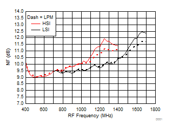
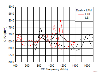
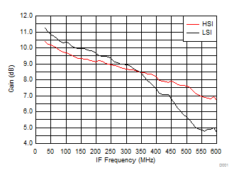
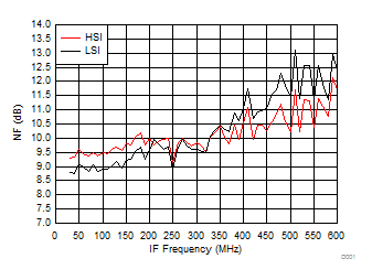
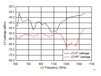
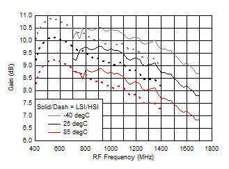
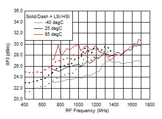
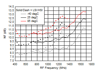
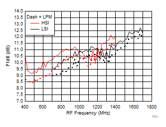
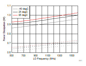
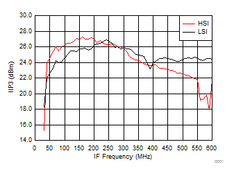
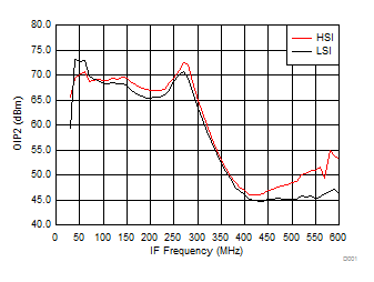
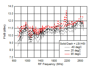
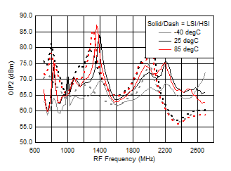
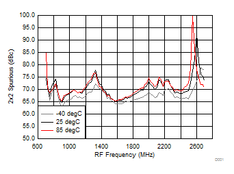
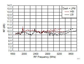
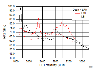
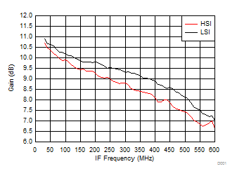
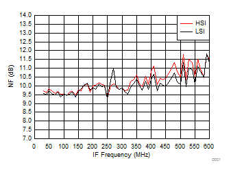
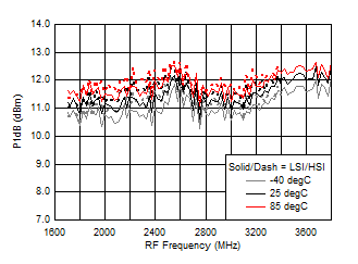
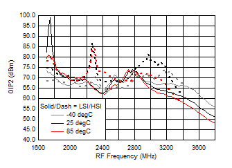
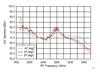
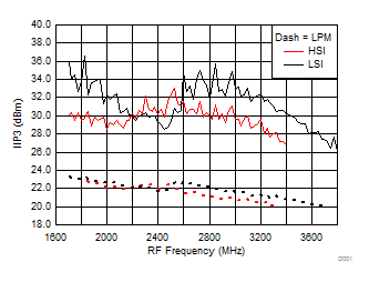
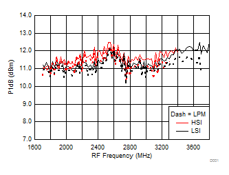
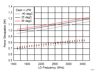
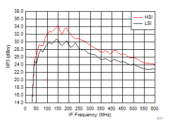
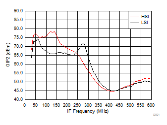
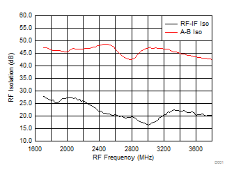
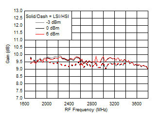
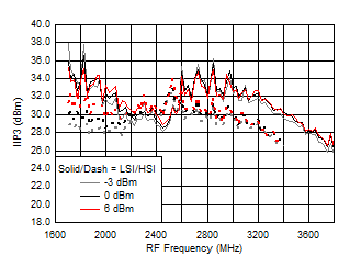
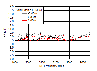
7.9 Typical Characteristics (TRF37A32)
TA = 25°C, VCC = 3.3 V; PRF = –10 dBm; FRF = 950 MHz; PLO = 0 dBm; FIF = 200 MHz; Low Side Injection, LPM = 0 (unless otherwise noted)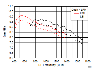
7.10 Typical Characteristics (TRF37B32)
TA = 25°C, VCC = 3.3 V; PRF = –10 dBm; FRF = 1950 MHz; PLO = 0 dBm; FIF = 200 MHz; Low Side Injection, LPM = 0 (unless otherwise noted)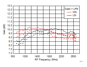
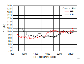
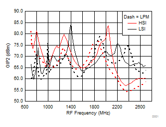
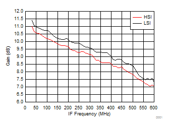
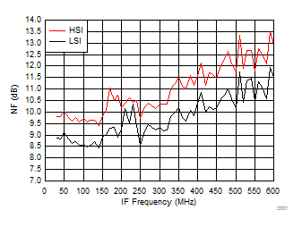
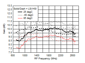
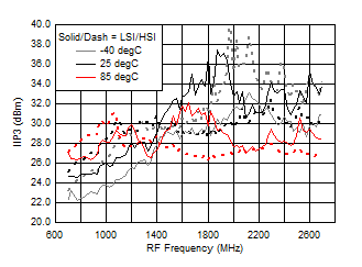
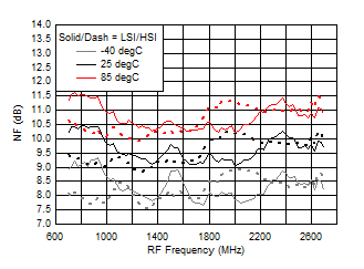
7.11 Typical Characteristics (TRF37C32)
TA = 25°C, VCC = 3.3 V; PRF = –10 dBm; FRF = 2500 MHz; PLO = 0 dBm; FIF = 200 MHz; Low Side Injection, LPM = 0 (unless otherwise noted)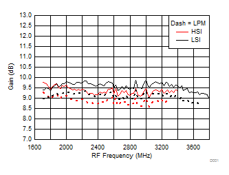
8 Detailed Description
8.1 Overview
The TRF37x32 family is a dual-channel, down convert receive mixer. It provides high-linearity over wide RF and IF bandwidths while also consuming low power. The device comes in three varieties, A, B, and C, to cover an extremely wide frequency band and can operate with either low side injection (LSI) or high side injection (HSI). The IF output is optimized for 200 MHz but operates from 30 MHz to 600 MHz with appropriate external components.
The device consists of a passive mixer core buffered by an LO amplifier and a high-linearity IF amplifier. There is an on-chip LDO to regulate VCC to the voltages needed for the small-geometry SiGe BiCMOS components. The single-ended RF and LO inputs each have a wideband internal balun. The balun's center tap is internally grounded.
Each channel offers an external power down terminal control which disables the IF circuitry. The device has a low power mode controlled through an external terminal control. Low power mode reduces bias current in the LO circuitry. Both power down and low power mode controls are internally biased to a normal operating state. The IFA/B_BT terminals are self-biased and require no external components.
The TRF37x32 uses a single 3.3 V power supply and draws exceptionally low current for its performance node.
8.2 Functional Block Diagram
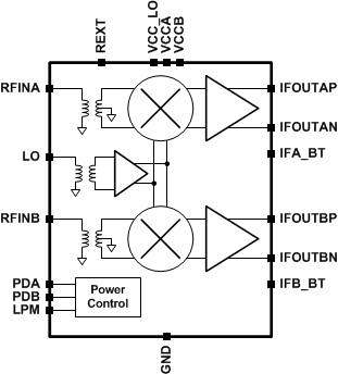 Figure 73. Block Diagram
8.3 Feature Description
8.3.1 Low Power Mode
Low power mode is enabled by setting the active-high LPM terminal to a logic high. The device contains an internal pull-down to engage normal operation when the terminal is left unconnected or floating.
Low power mode reduces the bias current in the LO amplifier portion of the device and affects both channels. Total current consumption is reduced 30% while lowering analog performance metrics.
8.3.2 Power Down
Each channel is powered down individually through the active-high PDA and PDB terminals. A logic high sets the respective channel in power down. The device contains an internal pull-down to engage normal operation when the terminal is left unconnected or floating.
Power down is implemented by removing bias in the IF amplifier. Operation of the opposite channel is not affected when either channel is turned off. Turn-on and turn-off time is fast enough to serve in most TDD applications.
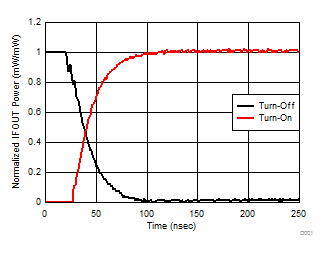 Figure 74. Device power down turn-on and turn-off time
8.3.3 Single Ended RF Input
Each RF input is single-ended with a wideband internal balun to convert the input to a differential signal, as shown in Figure 73. The center tap of the balun is internally grounded and is not available external to the device. The RF input should be ac coupled to driving circuitry according to the chart in Table 1.
Table 1. RF Input AC coupling capacitor
| Device | Blocking Cap Value |
|---|---|
| TRF37A32 | 20 pF |
| TRF37B32 | 10 pF |
| TRF37C32 | 10 pF |
8.3.4 Single Ended LO Input
The LO input is single ended with an internal balun to convert the input to a differential signal. The LO drive path includes a high frequency dual-mode oscillation inhibitor circuitry to ensure stable operation. For best operation it is recommended to keep the LO drive level at 0 dBm or higher to ensure inhibitor circuit does not falsely engage. At lower LO drive level, keep the LO power engaged to the device at power-up. At lower drive level the inhibitor may engage within certain frequency bands when the LO power transitions.
At the extreme RF frequencies the LO input bandwidth will force operation to either high side injection (HSI) or low side injection (LSI). Table 2 provides the operating range of the LO for each device.
Table 2. LO Input Frequency Operating Range
| Device | Operating Range | |
|---|---|---|
| TRF37A32 | 600 - 1400 MHz | |
| TRF37B32 | 500 - 2900 MHz | |
| TRF37C32 | Low Power mode (LPM) disabled | 1500 - 3600 MHz |
| Low Power mode (LPM) enabled | 1500 - 3500 MHz | |
8.3.5 IF Amplifier
The output of the device is driven by a high-linearity IF amplifier. The output nodes must be pulled up to VCC with high-Q inductors. It is designed to provide 200 Ω differential / 100 Ω single-ended output impedance. Layout should include symmetry for the differential output signal paths.
The IF output circuitry is optimized for performance at 200 MHz but operates over 30 MHz – 600 MHz.
8.4 Device Functional Modes
8.4.1 Low Power Mode
Low power mode is activated through the low power terminal, as described in the features description. It is designed for extremely low power consumption.
8.4.2 Single Channel and Shutdown Modes
The device may be operated as a single channel device by disabling one channel or in complete shutdown by disabling both channels.
