TRF37A73 1-6000 MHz RF Gain Block
1 Features
- 1 MHz – 6000 MHz
- Gain: 12 dB
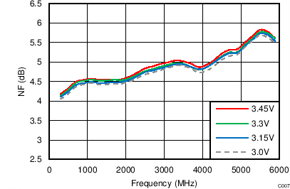
- Noise Figure: 4.5 dB
- Output P1dB: 14.5 dBm at 2000 MHz
- Output IP3: 28.5 dBm at 2000 MHz
- Power Down Mode
- Single Supply: 3.3 V
- Stabilized Performance Over Temperature
- Unconditionally Stable
- Robust ESD: >1 kV HBM; >1 kV CDM
2 Applications
- General Purpose RF Gain Block
- Consumer
- Industrial
- Utility Meters
- Low-cost Radios
- Cellular Base Station
- Wireless Infrastructure
- RF Backhaul
- Radar
- Electronic Warfare
- Software-defined Radio
- Test and Measurement
- Point-to-Point/Multipoint Microwave
- Software Defined Radios
- RF Repeaters
- Distributed Antenna Systems
- LO and PA Driver Amplifier
- Wireless Data, Satellite, DBS, CATV
- IF Amplifier
3 Description
The TRF37A73 is packaged in a 2.00mm x 2.00mm WSON with a power down pin feature making it ideal for applications where space and low power modes are critical.
The TRF37A73 is designed for ease of use. For maximum flexibility, this family of parts uses a common 3.3 V supply and consumes 55 mA. In addition, this family was designed with an active bias circuit that provides a stable and predictable bias current over process, temperature and voltage variations. For gain and linearity budgets the device was designed to provide a flat gain response and excellent OIP3 out to 6000 MHz. For space constrained applications, this family is internally matched to 50 Ω, which simplifies ease of use and minimizes needed PCB area.
Device Information(1)
| PART NUMBER | PACKAGE | BODY SIZE (NOM) |
|---|---|---|
| TRF37A73 | WSON (32) | 2.00mm x 2.00mm |
- For all available packages, see the orderable addendum at the end of the datasheet.
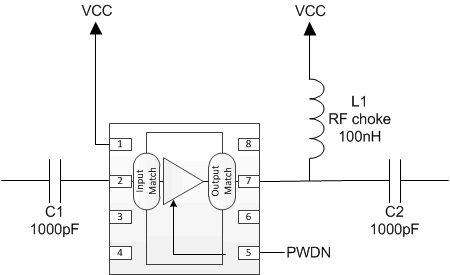
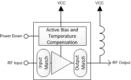
Simplified Schematic
4 Revision History
| DATE | REVISION | NOTES |
|---|---|---|
| May 2014 | * | Initial release. |
5 Pin Configuration and Functions
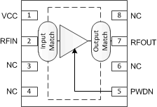
Pin Functions
| PIN | DESCRIPTION | |
|---|---|---|
| NAME | NO. | |
| VCC | 1 | DC Bias. |
| RFIN | 2 | RF input. Connect to an RF source through a DC-blocking capacitor. Internally matched to 50 Ω. |
| NC | 3, 4, 6, 8 | No electrical connection. Connect pad to GND for board level reliability integrity. |
| PWDN | 5 | When high the device is in power down state. When LOW or NC the device is in active state. Internal pulldown resistor to GND. |
| RFOUT | 7 | RF Output and DC Bias (VCC). Connect to DC supply through an RF choke inductor. Connect to output load through a DC-blocking capacitor. Internally matched to 50 Ω. |
| GND | PowerPAD™ | RF and DC GND. Connect to PCB ground plane. |
6 Specifications
6.1 Absolute Maximum Ratings
over operating free-air temperature range (unless otherwise noted) (1)| MIN | MAX | UNIT | ||
|---|---|---|---|---|
| Supply Input voltage | –0.3 | 3.6 | V | |
| Input Power | 10 | dBm | ||
| Operating virtual junction temperature range | –40 | 150 | °C | |
6.2 Handling Ratings
| MIN | MAX | UNIT | |||
|---|---|---|---|---|---|
| TSTG | Storage temperature range | –65 | 150 | °C | |
| VESD | Electrostatic discharge | Human body model (HBM), per ANSI/ESDA/JEDEC JS-001, all pins(1) | –1 | 1 | kV |
| Charged device model (CDM), per JEDEC specification JESD22-C101, all pins (2) | –1 | 1 | kV | ||
6.3 Recommended Operating Conditions
over operating free-air temperature range (unless otherwise noted)| MIN | NOM | MAX | UNIT | ||
|---|---|---|---|---|---|
| Supply Voltage, VCC | 3 | 3.3 | 3.45 | V | |
| Operating junction temperature, TJ | –40 | 125 | °C | ||
6.4 Thermal Information
| THERMAL METRIC(1) | DSG | UNIT | |
|---|---|---|---|
| 8 PINS | |||
| RθJA | Junction-to-ambient thermal resistance | 79.3 | °C/W |
| RθJCtop | Junction-to-case (top) thermal resistance | 110 | |
| RθJB | Junction-to-board thermal resistance | 49 | |
| ψJT | Junction-to-top characterization parameter | 6 | |
| ψJB | Junction-to-board characterization parameter | 49.4 | |
| RθJCbot | Junction-to-case (bottom) thermal resistance | 19.2 | |
6.5 Electrical Characteristics
VCC = 3V3, TA = 25°C, PWDN = Low, LOUT = 100 nH, C1 = C2 = 1000 pF, ZS = ZL = 50 Ω (unless otherwise noted)| PARAMETER | TEST CONDITIONS | MIN | TYP | MAX | UNIT | |
|---|---|---|---|---|---|---|
| DC PARAMETERS | ||||||
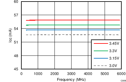
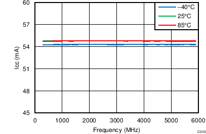
| ICC | Total supply current | 55 | 65 | mA | ||
| Power down current | PWDN = High | 125 | µA | |||
| Pdiss | Power dissipation | 0.182 | W | |||
| RF FREQUENCY RANGE | ||||||
| Frequency range | 1 | 6000 | MHz | |||
| G | Small signal gain | fRF = 400 MHz | 12.5 | dB | ||
| fRF = 2000 MHz | 12 | dB | ||||
| fRF = 3000 MHz | 11.5 | dB | ||||
| fRF = 4000 MHz | 11.5 | dB | ||||
| fRF = 5000 MHz | 11 | dB | ||||
| fRF = 6000 MHz | 10.5 | dB | ||||
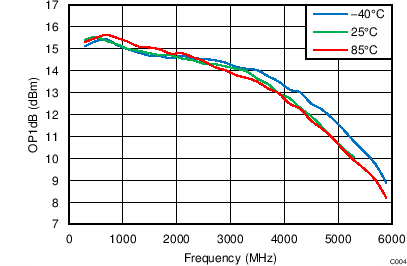
| OP1dB | Output 1dB compression point | At 2000 MHz | 14.5 | dBm | ||
| OIP3 | Output 3rd order intercept point | At 2000 MHz, 2-tone 10 MHz apart | 28.5 | dBm | ||
| NF | Noise figure | At 2000 MHz | 4.5 | dB | ||
| R(LI) | Input return loss | At 2000 MHz | 16 | dB | ||
| R(LO) | Output return loss | At 2000 MHz | 15 | dB | ||
| PWDN PIN | ||||||
| VIH | High level input level | 2 | V | |||
| VIL | Low level input level | 0.8 | V | |||
| IIH | High level input current | 30 | µA | |||
| IIL | Low level input current | 1 | µA | |||
6.6 Timing Requirements
| MIN | TYP | MAX | UNIT | |||
|---|---|---|---|---|---|---|
| PWDN PIN | ||||||
| tON | Turn-on Time | 50% TTL to 90% POUT | 0.6 | µs | ||
| tOFF | Turn-off Time | 50% TTL to 10% POUT | 1.4 | µs | ||
6.7 Typical Characteristics
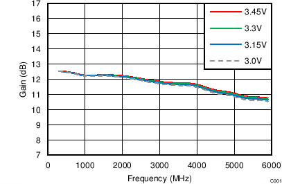
| VCC curves | Temp = 25°C | Pin = –10 dBm |
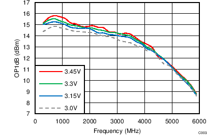
| VCC curves | Temp = 25°C |
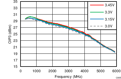
| VCC curves | Temp = 25°C | Pin = –10 dBm/tone |
| VCC curves | Temp = 25°C |
| VCC curves | Temp = 25°C |
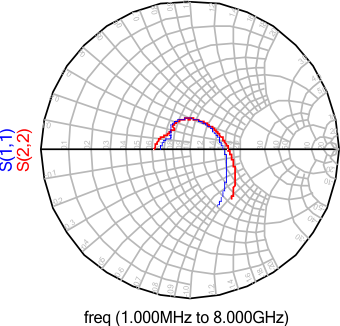
| VCC = 3.3 V | Temp = 25°C | 1 MHz to 8 GHz |
| Data Taken with EVM and Bias T, De-embedded to DUT pin | ||
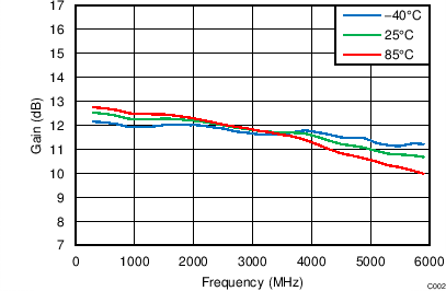
| Temp curves | VCC = 3.3 V | Pin = –10 dBm |
| Temp curves | VCC = 3.3 V |
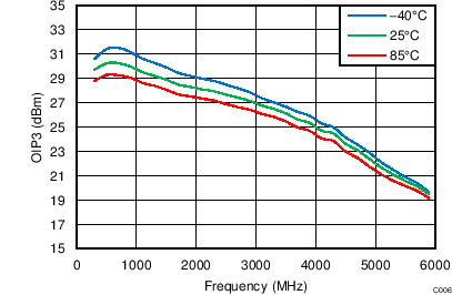
| Temp curves | VCC = 3.3 V | Pin = –10 dBm/tone |
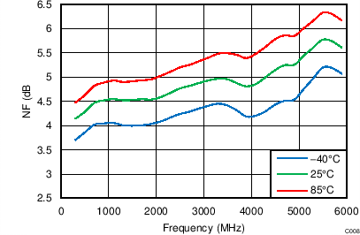
| Temp curves | VCC = 3.3 V |
| Temp curves | VCC = 3.3 V |
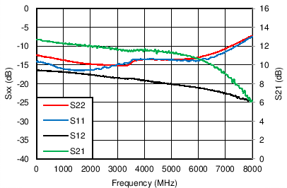
| VCC = 3.3 V | Temp = 25°C | 1 MHz to 8 GHz |
| Data Taken with EVM and Bias T, De-embedded to DUT pin | ||
7 Detailed Description
7.1 Overview
The device is a 3.3 V general purpose RF gain block. It is a SiGe Darlington amplifier with integrated 50 Ω input and output matching. The device contains an active bias circuit to maintain performance over a wide temperature and voltage range. The included power down function allows the amplifier to shut down saving power when the amplifier is not needed. Fast shut down and start up enable the amplifier to be used in a host of time division duplex applications.
7.2 Functional Block Diagram
7.3 Feature Description
The TRF37A73 is a fixed gain RF amplifier. It is internally matched to 50 Ω on both the input and output. It is a fully cascadable general purpose amplifier. The included active bias circuitry ensures the amplifier performance is optimized over the full operating temperature and voltage ranges.
7.4 Device Functional Modes
7.4.1 Power Down
The TRF37A73 PWDN pin can be left unconnected for normal operation or a logic-high for disable mode operation. For applications that use the power down mode, normal 5 V TLL levels are supported.
