SLOS732G June 2011 – March 2020 TRF7960A
PRODUCTION DATA.
- 1Device Overview
- 2Revision History
- 3Device Characteristics
- 4Terminal Configuration and Functions
- 5Specifications
-
6Detailed Description
- 6.1 Functional Block Diagram
- 6.2 Power Supplies
- 6.3 Supply Arrangements
- 6.4 Supply Regulator Settings
- 6.5 Power Modes
- 6.6 Receiver – Analog Section
- 6.7 Receiver – Digital Section
- 6.8 Oscillator Section
- 6.9 Transmitter - Analog Section
- 6.10 Transmitter - Digital Section
- 6.11 Transmitter – External Power Amplifier or Subcarrier Detector
- 6.12 Communication Interface
- 6.13
Direct Commands from MCU to Reader
- 6.13.1 Command Codes
- 6.13.2 Reset FIFO (0x0F)
- 6.13.3 Transmission With CRC (0x11)
- 6.13.4 Transmission Without CRC (0x10)
- 6.13.5 Delayed Transmission With CRC (0x13)
- 6.13.6 Delayed Transmission Without CRC (0x12)
- 6.13.7 Transmit Next Time Slot (0x14)
- 6.13.8 Block Receiver (0x16)
- 6.13.9 Enable Receiver (0x17)
- 6.13.10 Test Internal RF (RSSI at RX Input With TX On) (0x18)
- 6.13.11 Test External RF (RSSI at RX Input With TX Off) (0x19)
- 6.13.12 Register Preset
- 6.14
Register Description
- 6.14.1
Register Overview
- 6.14.1.1 Main Configuration Registers
- 6.14.1.2
Protocol Subsetting Registers
- 6.14.1.2.1 ISO14443B TX Options Register (0x02)
- 6.14.1.2.2 ISO14443A High-Bit-Rate and Parity Options Register (0x03)
- 6.14.1.2.3 TX Timer High Byte Control Register (0x04)
- 6.14.1.2.4 TX Timer Low Byte Control Register (0x05)
- 6.14.1.2.5 TX Pulse Length Control Register (0x06)
- 6.14.1.2.6 RX No Response Wait Time Register (0x07)
- 6.14.1.2.7 RX Wait Time Register (0x08)
- 6.14.1.2.8 Modulator and SYS_CLK Control Register (0x09)
- 6.14.1.2.9 RX Special Setting Register (0x0A)
- 6.14.1.2.10 Regulator and I/O Control Register (0x0B)
- 6.14.1.3 Status Registers
- 6.14.1.4 Test Registers
- 6.14.1.5 FIFO Control Registers
- 6.14.1
Register Overview
- 7Applications, Implementation, and Layout
- 8Device and Documentation Support
- 9Mechanical, Packaging, and Orderable Information
パッケージ・オプション
メカニカル・データ(パッケージ|ピン)
- RHB|32
サーマルパッド・メカニカル・データ
- RHB|32
発注情報
6.7.1.1 Internal RSSI – Main and Auxiliary Receivers
Each receiver path has its own RSSI block to measure the envelope of the demodulated RF signal (subcarrier). Internal Main RSSI and Internal Auxiliary RSSI are identical except that they are connected to different RF input pins. The Internal RSSI is intended for diagnostic purposes to set the correct RX path conditions.
The Internal RSSI values can be used to adjust the RX gain settings or decide which RX path (main or auxiliary) provides the greater amplitude and, hence, to decide if the MUX may need to be reprogrammed to swap the RX input signal. The measuring system latches the peak value, so the RSSI level can be read after the end of each receive packet. The RSSI register values are reset with every transmission (TX) by the reader. This guarantees an updated RSSI measurement for each new tag response.
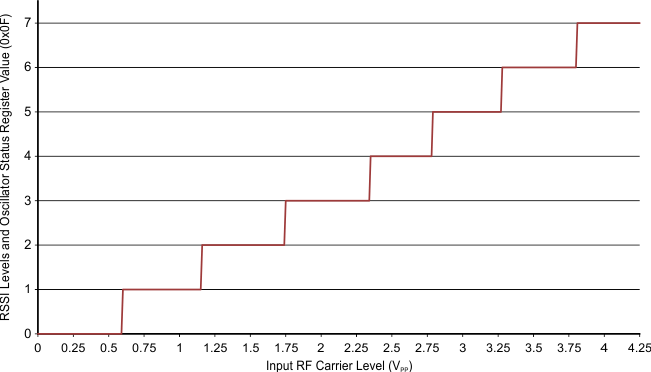
The Internal RSSI has 7 steps (3 bit) with a typical increment of approximately 4 dB. The operating range is 600 mVpp to 4.2 Vpp with a typical step size of approximately 600 mV. Both RSSI values "Internal Main" and "Internal Aux" RSSI are stored in the RSSI Levels and Oscillator Status register (0x0F).
Figure 6-2 shows the nominal relationship between the input RF peak level and the RSSI value.
 Figure 6-2 Digital Internal RSSI (Main and Auxiliary) Value vs RF Input Level
 This RSSI measurement is done during the communication to the Tag; this means the TX must be on. Bit 1 in the Chip Status Control register (0x00) defines if internal RSSI or the external RSSI value is stored in the RSSI Levels and Oscillator Status register 0x0F. Direct command 0x18 is used to trigger an internal RSSI measurement.