SLOS758G December 2011 – March 2020 TRF7963A
PRODUCTION DATA.
- 1Device Overview
- 2Revision History
- 3Device Characteristics
- 4Terminal Configuration and Functions
- 5Specifications
-
6Detailed Description
- 6.1 Functional Block Diagram
- 6.2 Power Supplies
- 6.3 Supply Arrangements
- 6.4 Supply Regulator Settings
- 6.5 Power Modes
- 6.6 Receiver – Analog Section
- 6.7 Receiver – Digital Section
- 6.8 Oscillator Section
- 6.9 Transmitter - Analog Section
- 6.10 Transmitter - Digital Section
- 6.11 Transmitter – External Power Amplifier or Subcarrier Detector
- 6.12 Communication Interface
- 6.13
Direct Commands from MCU to Reader
- 6.13.1 Command Codes
- 6.13.2 Reset FIFO (0x0F)
- 6.13.3 Transmission With CRC (0x11)
- 6.13.4 Transmission Without CRC (0x10)
- 6.13.5 Block Receiver (0x16)
- 6.13.6 Enable Receiver (0x17)
- 6.13.7 Test Internal RF (RSSI at RX Input With TX On) (0x18)
- 6.13.8 Test External RF (RSSI at RX Input With TX Off) (0x19)
- 6.13.9 Register Preset
- 6.14
Register Description
- 6.14.1
Register Overview
- 6.14.1.1 Main Configuration Registers
- 6.14.1.2
Protocol Subsetting Registers
- 6.14.1.2.1 ISO14443B TX Options Register (0x02)
- 6.14.1.2.2 ISO14443A High-Bit-Rate and Parity Options Register (0x03)
- 6.14.1.2.3 TX Pulse Length Control Register (0x06)
- 6.14.1.2.4 RX No Response Wait Time Register (0x07)
- 6.14.1.2.5 RX Wait Time Register (0x08)
- 6.14.1.2.6 Modulator and SYS_CLK Control Register (0x09)
- 6.14.1.2.7 RX Special Setting Register (0x0A)
- 6.14.1.2.8 Regulator and I/O Control Register (0x0B)
- 6.14.1.3 Status Registers
- 6.14.1.4 Test Registers
- 6.14.1.5 FIFO Control Registers
- 6.14.1
Register Overview
- 7Applications, Implementation, and Layout
- 8Device and Documentation Support
- 9Mechanical, Packaging, and Orderable Information
パッケージ・オプション
メカニカル・データ(パッケージ|ピン)
- RHB|32
サーマルパッド・メカニカル・データ
- RHB|32
発注情報
8.2 Device Nomenclature
To designate the stages in the product development cycle, TI assigns prefixes to the part numbers of devices. Each commercial family member has one of three prefixes: x, p, or no prefix. These prefixes represent evolutionary stages of product development from engineering prototypes (with prefix x) through fully qualified production devices (with no prefix).
Device development evolutionary flow:
xTRF... – Experimental device that is not necessarily representative of the electrical specifications of the final device
pTRF... – Final device that conforms to the electrical specifications of the final product but has not completed quality and reliability verification
TRF... – Fully qualified production device
Devices with a prefix of x or p are shipped against the following disclaimer:
"Developmental product is intended for internal evaluation purposes."
Production devices have been characterized fully, and the quality and reliability of the device have been demonstrated fully. TI's standard warranty applies.
Predictions show that prototype devices have a greater failure rate than the standard production devices. TI recommends that these devices not be used in any production system because their expected end-use failure rate still is undefined. Only qualified production devices are to be used.
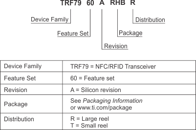
TI device nomenclature also includes a suffix with the device family name. This suffix indicates the package type and, optionally, the temperature range. Figure 8-1 provides a legend for reading the complete device name.
 Figure 8-1 Device Nomenclature