SLLS808A JULY 2007 – November 2016 TRS202
UNLESS OTHERWISE NOTED, this document contains PRODUCTION DATA.
- 1 Features
- 2 Applications
- 3 Description
- 4 Revision History
- 5 Pin Configuration and Functions
-
6 Specifications
- 6.1 Absolute Maximum Ratings
- 6.2 ESD Ratings
- 6.3 Recommended Operating Conditions
- 6.4 Thermal Information
- 6.5 Electrical Characteristics
- 6.6 Electrical Characteristics: Driver
- 6.7 Electrical Characteristics: Receiver
- 6.8 Switching Characteristics: Driver
- 6.9 Switching Characteristics: Receiver
- 6.10 Typical Characteristics
- 7 Parameter Measurement Information
- 8 Detailed Description
- 9 Application and Implementation
- 10Power Supply Recommendations
- 11Layout
- 12Device and Documentation Support
- 13Mechanical, Packaging, and Orderable Information
8 Detailed Description
8.1 Overview
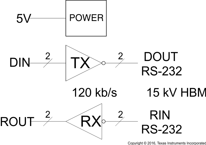
The TRS202 device is a dual driver and receiver that includes a capacitive voltage generator using four capacitors to supply TIA/EIA-232-F voltage levels from a single 5-V supply. Each receiver converts TIA/EIA-232-F inputs to 5-V TTL/CMOS levels. These receivers have shorted and open fail safe. The receiver can accept up to ±30-V inputs and decode inputs as low as ±3 V. Each driver converts TTL/CMOS input levels into TIA/EIA-232-F levels. Outputs are protected against shorts to ground.
8.2 Functional Block Diagram

8.3 Feature Description
8.3.1 Power
The power block increases and inverts the 5-V supply for the RS-232 driver using a charge pump that requires four 0.1-µF external capacitors.
8.3.2 RS-232 Driver
Two drivers interface standard logic levels to RS-232 levels. The driver inputs do not have internal pullup resistors. Do not float the driver inputs.
8.3.3 RS-232 Receiver
Two Schmitt trigger receivers interface RS-232 levels to standard logic levels. Each receiver has an internal 5-kΩ load to ground. An open input results in a high output on ROUT.
8.4 Device Functional Modes
8.4.1 VCC Powered by 5 V
The device is in normal operation when powered by 5 V.
8.4.2 VCC Unpowered
When TRS202 is unpowered, it can be safely connected to an active remote RS-232 device.
8.4.3 Truth Tables
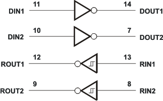
Table 1 and Table 2 list the function for each driver and receiver (respectively). Figure 9 shows the logic diagram.
Table 1. Function Table for Each Driver(1)
| INPUT DIN |
OUTPUT DOUT |
|---|---|
| L | H |
| H | L |
Table 2. Function Table for Each Receiver(1)
| INPUT RIN |
OUTPUT ROUT |
|---|---|
| L | H |
| H | L |
| Open | H |
Open = Input disconnected or connected driver off
 Figure 9. Logic Diagram (Positive Logic)