JAJSP98B August 2007 – October 2022 TRSF3243
PRODUCTION DATA
- 1特長
- 2アプリケーション
- 3概要
- 4Revision History
- 5Pin Configuration and Functions
-
6Specifications
- 6.1 Absolute Maximum Ratings
- 6.2 Recommended Operating Conditions
- 6.3 Thermal Information
- 6.4 Electrical Characteristics
- 6.5 Electrical Characteristics: Driver
- 6.6 Switching Characteristics: Driver
- 6.7 Electrical Characteristics: Receiver
- 6.8 Switching Characteristics: Receiver
- 6.9 Electrical Characteristics: Auto-Powerdown
- 6.10 Switching Characteristics: Auto-Powerdown
- 7Detailed Description
- 8Device and Documentation Support
- 9Mechanical, Packaging, and Orderable Information
パッケージ・オプション
メカニカル・データ(パッケージ|ピン)
サーマルパッド・メカニカル・データ
発注情報
Parameter Measurement Information
 Figure 7-1 Driver Slew Rate
 Figure 7-2 Driver Pulse Skew
 Figure 7-3 Receiver Propagation Delay Times
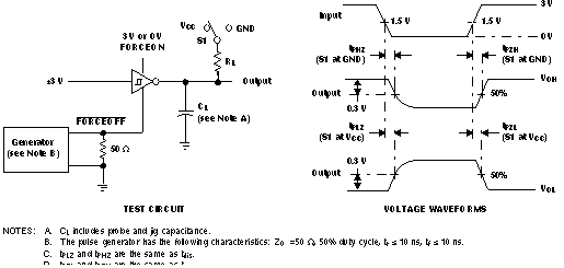
 Figure 7-4 Receiver Enable and Disable Times
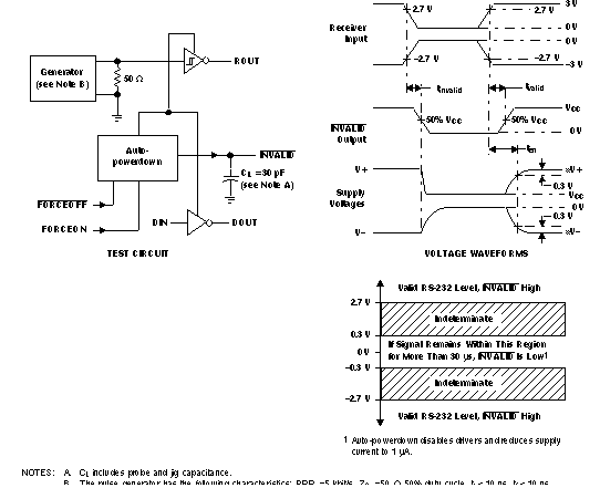
 Figure 7-5 INVALID Propagation Delay Times and Supply Enabling Time
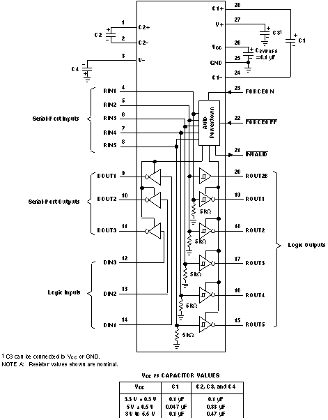
 Figure 7-6 Typical Operating Circuit and Capacitor Values