SCDS256A October 2009 – September 2016 TS3USB31E
PRODUCTION DATA.
- 1 Features
- 2 Applications
- 3 Description
- 4 Revision History
- 5 Pin Configuration and Functions
- 6 Specifications
- 7 Application Information
- 8 Parameter Measurement Information
- 9 Detailed Description
- 10Application and Implementation
- 11Power Supply Recommendations
- 12Layout
- 13Device and Documentation Support
- 14Mechanical, Packaging, and Orderable Information
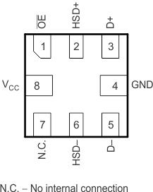
5 Pin Configuration and Functions
RSE Package
8-Pin UQFN
Top View

RSE Package
8-Pin UQFN
Bottom View

Pin Functions
| PIN | I/O | DESCRIPTION | |
|---|---|---|---|
| NAME | NO. | ||
| OE | 1 | I | Bus-switch enable, To isolate the D± pins from the HSD± pins set OE pin to valid high logic level, To connect D± pins to HSD± pins set OE pin to valid low logic level |
| D+ | 3 | I/O | Data ports |
| D– | 5 | I/O | Data ports |
| HSD+ | 2 | I/O | Data ports |
| HSD– | 6 | I/O | Data ports |
| N.C. | 7 | — | No connect, This pin must be left floating or connect to ground |
| GND | 4 | — | Ground |
| VCC | 8 | I/O | Supply voltage |