SCDS336C November 2012 – October 2016 TS5A3159-Q1
PRODUCTION DATA.
- 1 Features
- 2 Applications
- 3 Description
- 4 Revision History
- 5 Pin Configuration and Functions
-
6 Specifications
- 6.1 Absolute Maximum Ratings
- 6.2 ESD Ratings
- 6.3 Recommended Operating Conditions
- 6.4 Thermal Information
- 6.5 Electrical Characteristics for 5-V Supply
- 6.6 Electrical Characteristics for 3.3-V Supply
- 6.7 Electrical Characteristics For 2.5-V Supply
- 6.8 Electrical Characteristics For 1.8-V Supply
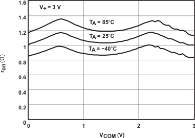
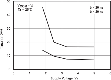
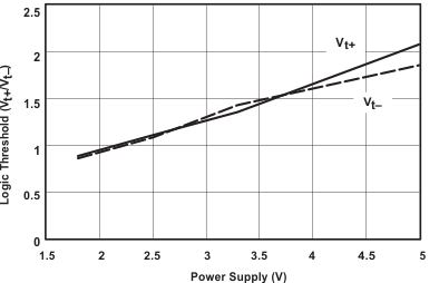
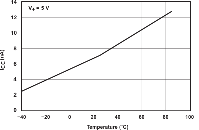
- 6.9 Typical Characteristics
- 7 Parameter Measurement Information
- 8 Detailed Description
- 9 Applications and Implementation
- 10Power Supply Recommendations
- 11Layout
- 12Device and Documentation Support
- 13Mechanical, Packaging, and Orderable Information
パッケージ・オプション
デバイスごとのパッケージ図は、PDF版データシートをご参照ください。
メカニカル・データ(パッケージ|ピン)
- DBV|6
サーマルパッド・メカニカル・データ
発注情報
6 Specifications
6.1 Absolute Maximum Ratings
over operating free-air temperature range (unless otherwise noted) (1)| MIN | MAX | UNIT | |||
|---|---|---|---|---|---|
| V+ | Supply voltage(2) | –0.5 | 6.5 | V | |
| VNO, VNC, VCOM | Analog voltage(2)(3)(4) | –0.5 | V+ + 0.5 | V | |
| II/OK | Analog port diode current | VNO, VNC, VCOM < 0 or VNO, VNC, VCOM > V+ | ±50 | mA | |
| INO, INC, ICOM | ON−state switch current | VNO, VNC, VCOM = 0 to V+ | ±200 | mA | |
| ON−state peak switch current(5) | ±400 | mA | |||
| VIN | Digital input voltage range(2)(3) | –0.5 | 6.5 | V | |
| IIK | Digital input clamp current | VIN < 0 | −50 | mA | |
| Continuous current through V+ or GND | ±100 | mA | |||
| TJ | Junction temperature | 150 | °C | ||
| Tstg | Storage temperature | –65 | 150 | °C | |
(1) Stresses beyond those listed under Absolute Maximum Ratings may cause permanent damage to the device. These are stress ratings only, and functional operation of the device at these or any other conditions beyond those indicated under Recommended Operating Conditions is not implied. Exposure to absolute-maximum-rated conditions for extended periods may affect device reliability.
(2) All voltages are with respect to ground, unless otherwise specified.
(3) The input and output voltage ratings may be exceeded if the input and output clamp-current ratings are observed.
(4) This value is limited to 5.5 V maximum.
(5) Pulse at 1 ms duration < 10% duty cycle.
6.2 ESD Ratings
| VALUE | UNIT | ||||
|---|---|---|---|---|---|
| V(ESD) | Electrostatic discharge | Human body model (HBM), per AEC Q100-002(1) | ±2000 | V | |
| Charged device model (CDM), per AEC Q100-011 | Corner pins (NO, NC, IN, and COM) | ±750 | |||
| Other pins | ±500 | ||||
(1) AEC Q100-002 indicates HBM stressing is done in accordance with the ANSI/ESDA/JEDEC JS-001 specification.
6.3 Recommended Operating Conditions
over operating free-air temperature range (unless otherwise noted)| MIN | MAX | UNIT | ||
|---|---|---|---|---|
| V+ | 1.65 | 5.5 | V | |
| IN | 0 | 5.5 | V | |
| NO, NC, COM | 0 | V+ | V | |
6.4 Thermal Information
| THERMAL METRIC(1) | TS5A3159-Q1 | UNIT | |
|---|---|---|---|
| DBV (SOT-23) | |||
| 6 PINS | |||
| RθJA | Junction-to-ambient thermal resistance | 192.9 | °C/W |
| RθJC(top) | Junction-to-case (top) thermal resistance | 133.3 | °C/W |
| RθJB | Junction-to-board thermal resistance | 37.6 | °C/W |
| ψJT | Junction-to-top characterization parameter | 38.9 | °C/W |
| ψJB | Junction-to-board characterization parameter | 37.1 | °C/W |
| RθJC(bot) | Junction-to-case (bottom) thermal resistance | N/A | °C/W |
(1) For more information about traditional and new thermal metrics, see the Semiconductor and IC Package Thermal Metrics application report.
6.5 Electrical Characteristics for 5-V Supply
V+ = 4.5 V to 5.5 V and TA = −40°C to +125°C (unless otherwise noted)| PARAMETER | TEST CONDITIONS | TA | V+ | MIN | TYP(1) | MAX | UNIT | ||
|---|---|---|---|---|---|---|---|---|---|
| ANALOG SWITCH | |||||||||
| VCOM, VNO,VNC | Analog signal range | 0 | V+ | V | |||||
| rpeak | Peak ON resistance | 0 ≤ VNO or VNC ≤ V+, ICOM = –30 mA |
Switch ON, See Figure 11 |
25°C | 4.5 V | 1 | 1.5 | Ω | |
| Full | 1.5 | ||||||||
| ron | ON-state resistance | VNO or VNC = 2.5 V, ICOM = –30 mA |
Switch ON, See Figure 10 |
25°C | 4.5 V | 0.75 | 1.3 | Ω | |
| Full | 1.3 | ||||||||
| ∆ron | ON-state resistance match between channels | VNO or VNC = 2.5 V, ICOM = –30 mA |
Switch ON, See Figure 10 |
25°C | 4.5 V | 0.1 | Ω | ||
| ron(flat) | ON-state resistance flatness | 0 ≤ VNO or VNC ≤ V+, ICOM = –30 mA |
Switch ON, See Figure 10 |
25°C | 4.5 V | 0.233 | Ω | ||
| VNO or VNC = 1 V, 1.5 V, 2.5 V, ICOM = –30 mA |
25°C | 0.15 | |||||||
| INC(OFF), INO(OFF) | NC, NO OFF leakage current |
VNC or VNO = 4.5 V, VCOM = 0 |
Switch OFF, See Figure 12 |
25°C | 5.5 V | −6 | 0.2 | 6 | nA |
| Full | −150 | 150 | |||||||
| INC(ON), INO(ON) | NC, NO ON leakage current |
VNC or VNO = 4.5 V, VCOM = Open |
Switch ON, See Figure 13 |
25°C | 5.5 V | −6 | 2.8 | 6 | nA |
| Full | −150 | 150 | |||||||
| ICOM(ON) | COM ON leakage current |
VNC or VNO = 4.5 V or Open, VCOM = 4.5 V |
Switch ON, See Figure 13 |
25°C | 5.5 V | –8 | 0.47 | 8 | nA |
| Full | −150 | 150 | |||||||
| DIGITAL INPUTS (IN) | |||||||||
| VIH | Input logic high | Full | 2.4 | 5.5 | V | ||||
| VIL | Input logic low | Full | 0 | 0.8 | V | ||||
| IIH, IIL | Input leakage current | VIN = 5.5 V or 0 | Full | 5.5 V | −1 | 1 | µA | ||
| DYNAMIC | |||||||||
| tON | Turn-on time | VCOM = V+, RL = 50 Ω, |
CL = 35 pF, See Figure 15 |
25°C | 4.5 V to 5.5 V | 20 | 35 | ns | |
| Full | 40 | ||||||||
| tOFF | Turn-off time | VCOM = V+, RL = 50 Ω, |
CL = 35 pF, See Figure 15 |
25°C | 4.5 V to 5.5 V | 15 | 20 | ns | |
| Full | 35 | ||||||||
| tBBM | Break-before-make time | VNC = VNO = V+ / 2, RL = 50 Ω, |
CL = 35 pF, See Figure 16 |
25°C | 4.5 V to 5.5 V | 1 | 12 | 14.5 | ns |
| Full | 1 | ||||||||
| QC | Charge injection | CL = 1 nF, VGEN = 0 V, | See Figure 19 | 25°C | 5 V | 36 | pC | ||
| CNC(OFF), CNO(OFF) | NC, NO OFF capacitance |
VNC or VNO = V+ or GND, Switch OFF, |
See Figure 13 | 25°C | 5 V | 23 | pF | ||
| CNC(ON), CNO(ON) | NC, NO ON capacitance |
VNC or VNO = V+ or GND, Switch ON, |
See Figure 13 | 25°C | 5 V | 84 | pF | ||
| CCOM(ON) | COM ON capacitance |
VCOM = V+ or GND, Switch ON, |
See Figure 13 | 25°C | 5 V | 84 | pF | ||
| CIN | Digital input capacitance | VIN = V+ or GND, | See Figure 13 | 25°C | 5 V | 2.1 | pF | ||
| BW | Bandwidth | RL = 50 Ω, Switch ON, |
See Figure 16 | 25°C | 5 V | 100 | MHz | ||
| OISO | OFF isolation | RL = 50 Ω, f = 1 MHz, |
Switch OFF, See Figure 17 |
25°C | 5 V | –65 | dB | ||
| XTALK | Crosstalk | RL = 50 Ω, f = 1 MHz, |
Switch ON, See Figure 18 |
25°C | 5 V | –65 | dB | ||
| THD | Total harmonic distortion | RL = 600 Ω, CL = 50 pF, |
f = 600 Hz to 20 kHz, See Figure 19 |
25°C | 5 V | 0.01% | |||
| SUPPLY | |||||||||
| I+ | Positive supply current | VIN = V+ or GND, | Switch ON or OFF | 25°C | 5.5 V | 0.1 | µA | ||
| Full | 0.5 | ||||||||
(1) TA = 25°C
6.6 Electrical Characteristics for 3.3-V Supply
V+ = 3 V to 3.6 V and TA = −40°C to +125°C (unless otherwise noted)| PARAMETER | TEST CONDITIONS | TA | V+ | MIN | TYP(1) | MAX | UNIT | ||
|---|---|---|---|---|---|---|---|---|---|
| ANALOG SWITCH | |||||||||
| VCOM, VNO,VNC | Analog signal range | 0 | V+ | V | |||||
| rpeak | Peak ON-state resistance | 0 ≤ VNO or VNC ≤ V+, ICOM = –24 mA, |
Switch ON, See Figure 10 |
25°C | 3 V | 1.35 | 2.2 | Ω | |
| Full | 2.2 | ||||||||
| ron | ON-state resistance | VNO or VNC = 2 V, ICOM = –24 mA, |
Switch ON, See Figure 10 |
25°C | 3 V | 1.15 | 1.8 | Ω | |
| Full | 1.8 | ||||||||
| ∆ron | ON-state resistance match between channels | VNO or VNC = 2 V, 0.8 V, ICOM = –24 mA, |
Switch ON, See Figure 10 |
25°C | 3 V | 0.11 | Ω | ||
| ron(flat) | ON-state resistance flatness | 0 ≤ VNO or VNC ≤ V+, ICOM = –24 mA, |
Switch ON, See Figure 10 |
25°C | 3 V | 0.225 | Ω | ||
| VNO or VNC = 2 V, 0.8 V, ICOM = –24 mA, |
25°C | 0.25 | |||||||
| INC(OFF), INO(OFF) |
NC, NO OFF leakage current |
VNC or VNO = 3 V, VCOM = 0, |
Switch OFF, See Figure 11 |
25°C | 3.6 V | 0.2 | nA | ||
| INC(ON), INO(ON) |
NC, NO ON leakage current |
VNC or VNO = 3 V, VCOM = Open, |
Switch ON, See Figure 12 |
25°C | 3.6 V | 2.8 | nA | ||
| ICOM(ON) | COM ON leakage current |
VNC or VNO = 3 V or Open, VCOM = 3 V, |
Switch ON, See Figure 12 |
25°C | 3.6 V | 0.47 | nA | ||
| DIGITAL INPUTS (IN) | |||||||||
| VIH | Input logic high | Full | 2 | 5.5 | V | ||||
| VIL | Input logic low | Full | 0 | 0.6 | V | ||||
| IIH, IIL | Input leakage current | VIN = 5.5 V or 0 | Full | 3.6 V | –1 | 1 | µA | ||
| DYNAMIC | |||||||||
| tON | Turn-on time | VCOM = V+, RL = 50 Ω |
CL = 35 pF, See Figure 15 |
25°C | 3 V to 3.6 V | 30 | 40 | ns | |
| Full | 55 | ||||||||
| tOFF | Turn-off time | VCOM = V+, RL = 50 Ω |
CL = 35 pF, See Figure 15 |
25°C | 3 V to 3.6 V | 20 | 25 | ns | |
| Full | 40 | ||||||||
| tBBM | Break-before-make time | VNC = VNO = V+ / 2, RL = 50 Ω |
CL = 35 pF, See Figure 16 |
25°C | 3 V to 3.6 V | 1 | 21 | 29 | ns |
| Full | 1 | ||||||||
| QC | Charge injection | CL = 1 nF, VGEN = 0 V | See Figure 19 | 25°C | 3.3 V | 20 | pC | ||
| CNC(OFF), CNO(OFF) | NC, NO OFF capacitance | VNC or VNO = V+ or GND, Switch OFF |
See Figure 13 | 25°C | 3.3 V | 23 | pF | ||
| CNC(ON), CNO(ON) | NC, NO ON capacitance | VNC or VNO = V+ or GND, Switch ON |
See Figure 13 | 25°C | 3.3 V | 84 | pF | ||
| CCOM(ON) | COM ON capacitance | VCOM = V+ or GND, Switch ON |
See Figure 13 | 25°C | 3.3 V | 84 | pF | ||
| CIN | Digital input capacitance | VIN = V+ or GND | See Figure 13 | 25°C | 3.3 V | 2.1 | pF | ||
| BW | Bandwidth | RL = 50 Ω, Switch ON |
See Figure 16 | 25°C | 3.3 V | 100 | MHz | ||
| OISO | OFF isolation | RL = 50 Ω, f = 1 MHz |
Switch OFF, See Figure 17 |
25°C | 3.3 V | –65 | dB | ||
| XTALK | Crosstalk | RL = 50 Ω, f = 1 MHz |
Switch ON, See Figure 18 |
25°C | 3.3 V | –65 | dB | ||
| THD | Total harmonic distortion | RL = 600 Ω, CL = 50 pF |
f = 600 Hz to 20 kHz, See Figure 19 |
25°C | 3.3 V | 0.015% | |||
| SUPPLY | |||||||||
| I+ | Positive supply current | VIN = V+ or GND | Switch ON or OFF | 25°C | 3.6 V | 0.1 | μA | ||
| Full | 0.5 | ||||||||
(1) TA = 25°C
6.7 Electrical Characteristics For 2.5-V Supply
V+ = 2.3 V to 2.7 V and TA = −40°C to +125°C (unless otherwise noted)| PARAMETER | TEST CONDITIONS | TA | V+ | MIN | TYP(1) | MAX | UNIT | ||
|---|---|---|---|---|---|---|---|---|---|
| ANALOG SWITCH | |||||||||
| VCOM, VNO,VNC | Analog signal range | 0 | V+ | V | |||||
| rpeak | Peak ON-state resistance | 0 ≤ VNO or VNC ≤ V+, ICOM = –8 mA |
Switch ON, See Figure 10 |
25°C | 2.5 V | 1.7 | 2.9 | Ω | |
| Full | 2.9 | ||||||||
| ron | ON-state resistance | VNO or VNC = 1.8 V, ICOM = –8 mA |
Switch ON, See Figure 10 |
25°C | 2.5 V | 1.45 | 2.3 | Ω | |
| Full | 2.3 | ||||||||
| ∆ron | ON-state resistance match between channels | VNO or VNC = 0.8 V, 1.8 V, ICOM = –8 mA |
Switch ON, See Figure 10 |
25°C | 2.5 V | 0.7 | Ω | ||
| ron(flat) | ON-state resistance flatness | 0 ≤ VNO or VNC ≤ V+, ICOM = –8 mA |
Switch ON, See Figure 10 |
25°C | 2.5 V | 0.5 | Ω | ||
| VNO or VNC = 0.8 V, 1.8 V, ICOM = –8 mA |
25°C | 0.45 | |||||||
| INC(OFF), INO(OFF) | NC, NO Off leakage current |
VNC or VNO = 2.3 V, VCOM = 0 |
Switch OFF, See Figure 11 |
25°C | 2.7 V | 0.2 | nA | ||
| INC(ON), INO(ON) | NC, NO On leakage current |
VNC or VNO = 2.3 V, VCOM = Open |
Switch ON, See Figure 12 |
25°C | 2.7 V | 2.8 | nA | ||
| ICOM(ON) | COM On leakage current |
VNC or VNO = 2.3 V or Open, VCOM = 2.3 V |
Switch ON, See Figure 12 |
25°C | 2.7 V | 0.47 | nA | ||
| DIGITAL INPUTS (IN) | |||||||||
| VIH | Input logic high | Full | 1.8 | 5.5 | V | ||||
| VIL | Input logic low | Full | 0 | 0.6 | V | ||||
| IIH, IIL | Input leakage current | VIN = 5.5 V or 0 | Full | 2.7 V | −1 | 1 | µA | ||
| DYNAMIC | |||||||||
| tON | Turn-on time | VCOM = V+, RL = 50 Ω, |
CL = 35 pF, See Figure 15 |
25°C | 2.3 V to 2.7 V | 40 | 55 | ns | |
| Full | 70 | ||||||||
| tOFF | Turn-off time | VCOM = V+, RL = 50 Ω, |
CL = 35 pF, See Figure 15 |
25°C | 2.3 V to 2.7 V | 30 | 40 | ns | |
| Full | 55 | ||||||||
| tBBM | Break-before-make time | VNC = VNO = V+ / 2, RL = 50 Ω, |
CL = 35 pF, See Figure 16 |
25°C | 2.3 V to 2.7 V | 1 | 33 | 39 | ns |
| Full | 1 | ||||||||
| QC | Charge injection | CL = 1 nF, VGEN = 0 V, | See Figure 19 | 25°C | 2.5 V | 13 | pC | ||
| CNC(OFF), CNO(OFF) |
NC, NO OFF capacitance |
VNC or VNO = V+ or GND, Switch OFF, |
See Figure 14 | 25°C | 2.5 V | 23 | pF | ||
| CNC(ON), CNO(ON) |
NC, NO ON capacitance |
VNC or VNO = V+ or GND, Switch ON, |
See Figure 14 | 25°C | 2.5 V | 84 | pF | ||
| CCOM(ON) | COM ON capacitance |
VCOM = V+ or GND, Switch ON, |
See Figure 14 | 25°C | 2.5 V | 84 | pF | ||
| CIN | Digital input capacitance | VIN = V+ or GND, | See Figure 14 | 25°C | 2.5 V | 2.1 | pF | ||
| BW | Bandwidth | RL = 50 Ω, Switch ON, |
See Figure 16 | 25°C | 2.5 V | 100 | MHz | ||
| OISO | OFF isolation | RL = 50 Ω, f = 1 MHz, |
Switch OFF, See Figure 17 |
25°C | 2.5 V | –64 | dB | ||
| XTALK | Crosstalk | RL = 50 Ω, f = 1 MHz, |
Switch ON, See Figure 18 |
25°C | 2.5 V | –64 | dB | ||
| THD | Total harmonic distortion | RL = 600 Ω, CL = 50 pF, |
f = 600 Hz to 20 kHz, See Figure 19 |
25°C | 2.5 V | 0.025% | |||
| SUPPLY | |||||||||
| I+ | Positive supply current | VIN = V+ or GND, | Switch ON or OFF | 25°C | 2.7 V | 0.1 | μA | ||
| Full | 0.5 | ||||||||
(1) TA = 25°C
6.8 Electrical Characteristics For 1.8-V Supply
V+ = 1.65 V to 1.95 V and TA = −40°C to +125°C (unless otherwise noted| PARAMETER | TEST CONDITIONS | TA | V+ | MIN | TYP(1) | MAX | UNIT | ||
|---|---|---|---|---|---|---|---|---|---|
| ANALOG SWITCH | |||||||||
| VCOM, VNO,VNC | Analog signal range | 0 | V+ | V | |||||
| rpeak | Peak ON-state resistance |
0 ≤ VNO or VNC ≤ V+, ICOM = −2 mA |
Switch ON, See Figure 10 |
25°C | 1.8 V | 4 | 5.2 | Ω | |
| Full | 5.2 | ||||||||
| ron | ON-state resistance | VNO or VNC = 1.5 V, ICOM = −2 mA |
Switch ON, See Figure 10 |
25°C | 1.8 V | 1.7 | 3.5 | Ω | |
| Full | 3.5 | ||||||||
| ∆ron | ON-state resistance match between channels | VNO or VNC = 0.6 V, 1.5 V, ICOM = −2 mA |
Switch ON, See Figure 10 |
25°C | 1.8 V | 0.7 | Ω | ||
| Full | 0.7 | ||||||||
| ron(flat) | ON-state resistance flatness | 0 ≤ VNO or VNC ≤ V+, ICOM = −2 mA |
Switch ON, See Figure 11 |
25°C | 1.8 V | 1.85 | Ω | ||
| Full | 1.85 | ||||||||
| VNO or VNC = 0.6 V, 1.5 V, ICOM = −2 mA |
25°C | 0.9 | |||||||
| Full | 0.9 | ||||||||
| INC(OFF), INO(OFF) | NC, NO Off leakage current |
VNC or VNO = 1.65 V, VCOM = 0 |
Switch OFF, See Figure 11 |
25°C | 1.95 V | 0.2 | nA | ||
| INC(ON), INO(ON) | NC, NO On leakage current |
VNC or VNO = 1.65 V, VCOM = Open |
Switch ON, See Figure 12 |
25°C | 1.95 V | 2.8 | nA | ||
| ICOM(ON) | COM On leakage current |
VNC or VNO = 1.65 V or Open, VCOM = 1.65 V |
Switch ON, See Figure 12 |
25°C | 1.95 V | 0.47 | nA | ||
| DIGITAL INPUTS (IN) | |||||||||
| VIH | Input logic high | Full | 1.5 | 5.5 | V | ||||
| VIL | Input logic low | Full | 0 | 0.6 | V | ||||
| IIH, IIL | Input leakage current | VIN = 5.5 V or 0 | Full | 1.95 V | −1 | 1 | µA | ||
| DYNAMIC | |||||||||
| tON | Turn-on time | VCOM = V+, RL = 50 Ω, |
CL = 35 pF, See Figure 15 |
25°C | 1.65 V to 1.95 V | 65 | 70 | ns | |
| Full | 95 | ||||||||
| tOFF | Turn-off time | VCOM = V+, RL = 50 Ω, |
CL = 35 pF, See Figure 15 |
25°C | 1.65 V to 1.95 V | 40 | 55 | ns | |
| Full | 70 | ||||||||
| tBBM | Break-before-make time | VNC = VNO = V+ / 2, RL = 50 Ω, |
CL = 35 pF, See Figure 15 |
25°C | 1.65 V to 1.95 V | 1 | 60 | 72 | ns |
| Full | 0.5 | ||||||||
| QC | Charge injection | CL = 1 nF, VGEN = 0 V, | See Figure 19 | 25°C | 1.8 V | 13 | pC | ||
| CNC(OFF), CNO(OFF) |
NC, NO OFF capacitance |
VNC or VNO = V+ or GND, Switch OFF, |
See Figure 14 | 25°C | 1.8 V | 23 | pF | ||
| CNC(ON), CNO(ON) |
NC, NO ON capacitance |
VNC or VNO = V+ or GND, Switch ON, |
See Figure 14 | 25°C | 1.8 V | 84 | pF | ||
| CCOM(ON) | COM ON capacitance |
VCOM = V+ or GND, Switch ON, |
See Figure 14 | 25°C | 1.8 V | 84 | pF | ||
| CIN | Digital input capacitance | VIN = V+ or GND, | See Figure 14 | 25°C | 1.8 V | 2.1 | pF | ||
| BW | Bandwidth | RL = 50 Ω, Switch ON, |
See Figure 16 | 25°C | 1.8 V | 100 | MHz | ||
| OISO | OFF isolation | RL = 50 Ω, f = 1 MHz, |
Switch OFF, See Figure 17 |
25°C | 1.8 V | –63 | dB | ||
| XTALK | Crosstalk | RL = 50 Ω, f = 1 MHz, |
Switch ON, See Figure 18 |
25°C | 1.8 V | –63 | dB | ||
| SUPPLY | |||||||||
| I+ | Positive supply current | VIN = V+ or GND, | Switch ON or OFF | 25°C | 1.95 V | 0.1 | μA | ||
| Full | 0.5 | ||||||||
(1) TA = 25°C
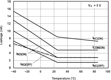
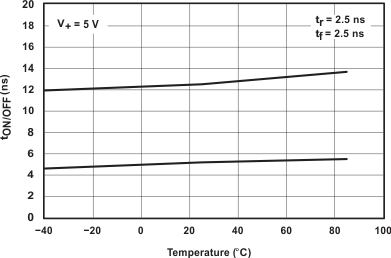
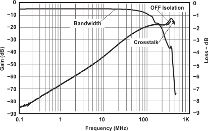
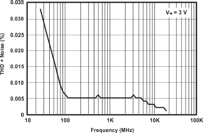
6.9 Typical Characteristics
