SCDS203B DECEMBER 2005 – March 2019 TS5A63157
PRODUCTION DATA.
- 1 Features
- 2 Applications
- 3 Description
- 4 Revision History
- 5 Pin Configuration and Functions
-
6 Specifications
- 6.1 Absolute Minimum and Maximum Ratings
- 6.2 ESD Ratings
- 6.3 Recommended Operating Conditions
- 6.4 Thermal Information
- 6.5 Electrical Characteristics for 5-V Supply
- 6.6 Electrical Characteristics for 3.3-V Supply
- 6.7 Electrical Characteristics for 2.5-V Supply
- 6.8 Electrical Characteristics for 1.8-V Supply
- 6.9 Typical Characteristics
- 7 Parameter Measurement Information
- 8 Detailed Description
- 9 Application and Implementation
- 10Power Supply Recommendations
- 11Layout
- 12Device and Documentation Support
- 13Mechanical, Packaging, and Orderable Information
パッケージ・オプション
メカニカル・データ(パッケージ|ピン)
サーマルパッド・メカニカル・データ
発注情報
6.9 Typical Characteristics
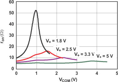
 Figure 1. ron vs VCOM
  Figure 3. ron vs VCOM (V+ = 5 V)
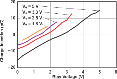
  Figure 5. Charge Injection (QC) vs VCOM
  Figure 7. tON and tOFF vs Temperature (V+ = 5 V)
  Figure 9. Bandwidth (V+ = 3.3 V)
  Figure 11. Total Harmonic Distortion (THD) vs Frequency (V+ = 3.3 V)
  Figure 2. ron vs VCOM (V+ = 3 V)
  Figure 4. Leakage Current vs Temperature (V+ = 5.5 V)
  Figure 6. tON and tOFF vs Supply Voltage
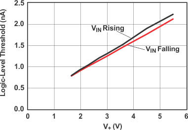
  Figure 8. Logic-Level Threshold vs V+
  Figure 10. OFF Isolation and Crosstalk (V+ = 3.3 V)
  Figure 12. Power-Supply Current vs Temperature (V+ = 5 V)