JAJSEK0B January 2018 – July 2018 TS5MP645
PRODUCTION DATA.
- 1 特長
- 2 アプリケーション
- 3 概要
- 4 改訂履歴
- 5 Pin Configuration and Functions
- 6 Specifications
- 7 Parameter Measurement Information
- 8 Detailed Description
- 9 Application and Implementation
- 10Power Supply Recommendations
- 11Layout
- 12デバイスおよびドキュメントのサポート
- 13メカニカル、パッケージ、および注文情報
パッケージ・オプション
デバイスごとのパッケージ図は、PDF版データシートをご参照ください。
メカニカル・データ(パッケージ|ピン)
- YFP|36
サーマルパッド・メカニカル・データ
発注情報
7 Parameter Measurement Information
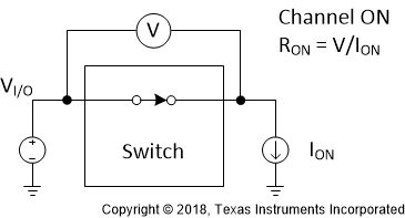 Figure 7. On Resistance
  Figure 8. Off Leakage
  Figure 9. On Leakage
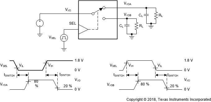
1. All input pulses are supplied by generators having the following characteristics: PRR ≤ 10 MHz, ZO = 50 Ω , tr = 3 ns, tf = 3 ns.
2. CL includes probe and jig capacitance.
Figure 10. tSWITCH timing 
1. All input pulses are supplied by generators having the following characteristics: PRR ≤ 10 MHz, ZO = 50 Ω , tr = 3 ns, tf = 3 ns.
2. CL includes probe and jig capacitance.
Figure 11. tON and tOFF Timing for OE 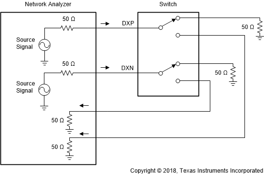 Figure 12. Off Isolation
 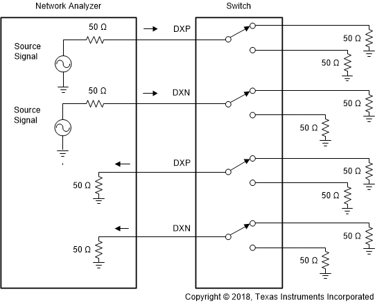 Figure 13. Crosstalk
 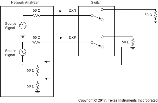 Figure 14. BW and Insertion Loss
 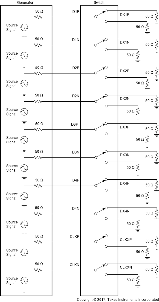 Figure 15. tPD, tSKEW(INTRA) and tSKEW Setup
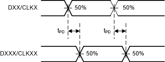
1. All input pulses are supplied by generators having the following characteristics: PRR ≤ 10 MHz, ZO = 50 Ω , tr = 100 ps, tf = 100 ps.
2. CL includes probe and jig capacitance.
Figure 16. tPD 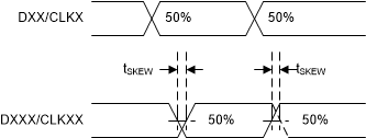
1. All input pulses are supplied by generators having the following characteristics: PRR ≤ 10 MHz, ZO = 50 Ω , tr = 100 ps, tf = 100 ps.
2. CL includes probe and jig capacitance.
Figure 17. tSKEW 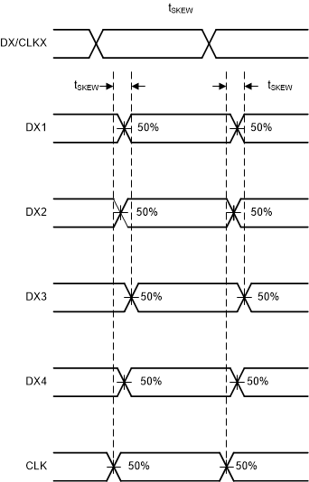
1. All input pulses are supplied by generators having the following characteristics: PRR ≤ 10 MHz, ZO = 50 Ω , tr = 100 ps, tf = 100 ps.
2. CL includes probe and jig capacitance.
3. tSK(INTER) is the max skew between all channels. Diagram exaggerates tSK(INTER) to show measurement technique
Figure 18. tSKEW 
1. All input pulses are supplied by generators having the following characteristics: PRR ≤ 10 MHz, ZO = 50 Ω , tr = 3 ns, tf = 3 ns.
2. CL includes probe and jig capacitance.
Figure 19. tBBM