SLLS783C May 2009 – March 2016 TSB81BA3E
PRODUCTION DATA.
- 1 Features
- 2 Description
- 3 Revision History
- 4 Description Continued
- 5 Pin Configuration and Function
- 6 Electrical Specfications
- 7 Parameter Measurement Information
- 8 Detailed Description
- 9 Application and Implementation
- 10Power Supply Recommendations
- 11Layout
- 12Device and Documentation Support
- 13Mechanical, Packaging, and Orderable Information
9 Application and Implementation
NOTE
Information in the following applications sections is not part of the TI component specification, and TI does not warrant its accuracy or completeness. TI’s customers are responsible for determining suitability of components for their purposes. Customers should validate and test their design implementation to confirm system functionality.
9.1 Application Information
The TSB81BA3E provides the digital and analog transceiver functions needed to implement a three-port node in a cable-based IEEE 1394 network. Each cable port incorporates two differential line Interface (HCI) Requirements transceivers. The transceivers include circuitry to monitor the line conditions as needed for determining connection status, for initialization and arbitration, and for packet reception and transmission.
9.2 Typical Application
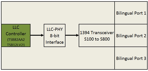
A common application of the TSB81BA3E is a three-port 1394 transceiver, it can be configured port-basis for data strobe only, beta mode or bilingual modes.
 Figure 9. 3-Port 1394 Transceiver in 1394b Mode
9.2.1 Design Requirements
For this design example, use the parameters shown in Table 12.
Table 12. Design Parameters
| PARAMETER | EXAMPLE VALUE |
|---|---|
| PHY POWER | 3.3 V |
| LLC Controller | TSB82AA2 |
| Crystal | 24.576 MHz |
| Downstream Ports | 3- 1394 Bilingual |
| Power Class | PC[0:2] = 100 |
| Bus Power | 12 V |
9.2.2 Detailed Design Procedure
9.2.2.1 Port Termination for a 1394 Bilingual Port
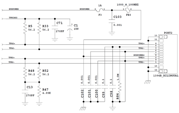
The TPA and TPB lines require termination as illustrated in the following figure, the 1394 node connecting to this external port shall have the same terminations on its ports.
When configuring the TSB81BA3E port to be data-strobe only the TPBIAS terminal can be left unconnected.
 Figure 10. Port Termination
9.2.2.2 PHY-LINK Interface
The PHY-link interface of the TSB81BA3E can follow either the 1394a protocol or the 1394b protocol. When using any 1394-1995 or 1394a links such as the TSB12LV01B or the TSB12LV32, the PHY-link interface has to be in the 1394a protocol. In this case, the BMODE pin has to be tied low to GND.
When using any 1394b link such as the TSB82AA2, the PHY-link interface has to be in the 1394b protocol. In this case, the BMODE pin is tied high. The BMODE pin only sets the mode of operation of the PHY-link interface; it does not set the mode of operation of the cable interface. No isolation is implemented in this schematic.
The PHY and link operate off of the same ground plane. To reduce EMI emissions and reduce reflections on the PCLK line, a series-damping resistor is recommended. The schematic shows a 0-Ω resistor, which is essentially a placeholder on the board. To reduce EMI, a 22-Ω resistor on the PCLK line is recommended. This resistor should be placed as close to the PHY as possible. Its value can be adjusted to reduce emissions. By slowing down the edge rates on PCLK, this 22-Ω resistor significantly reduces reflections that may occur when the distance between the PHY and link is large (greater than 4 inches in this case).
The Link Request signal (LREQ) is input to the PHY from the link. The link uses this to initiate a service request to the PHY. When the BMODE pin is deasserted, the IEEE 1394b-2002 BOSS arbitration is disabled and the LREQ request stream follows the 1394a specification.
If a power down option control for PD is not implemented, the PD pin on the PHY (pin 77) should be tied to ground through a 1-kΩ resistor to keep the PHY enabled.