SLLS783C May 2009 – March 2016 TSB81BA3E
PRODUCTION DATA.
- 1 Features
- 2 Description
- 3 Revision History
- 4 Description Continued
- 5 Pin Configuration and Function
- 6 Electrical Specfications
- 7 Parameter Measurement Information
- 8 Detailed Description
- 9 Application and Implementation
- 10Power Supply Recommendations
- 11Layout
- 12Device and Documentation Support
- 13Mechanical, Packaging, and Orderable Information
11 Layout
11.1 Layout Guidelines
Put pads in for all components in prototype boards. When testing prototype boards for EMI and ESD, some of the following components may not be required:
- The 1394 connector gasket between chassis GND, 1394 connector shield, and metal bracket on PCB board (for example on a PCI add-in card).
- The ferrite on the cable V- ground pin (socket pin 2).
- The ferrite on the cable V+ power pin (socket pin 1).
11.1.1 Board Stackup
Because of the high frequencies associated with 1394, a 1394 board with at least four layers is recommended; two signal layers separated by a ground and power layer (See Figure 12).
 Figure 12. Four-Layer Board Stackup
The majority of signal traces should be run on a single layer, preferably SIGNAL1. Immediately next to this layer should be the GND plane which is solid with no cuts. Avoid running signal traces across a split in the ground or power plane. When running across split planes is unavoidable, sufficient decoupling must be used (see Section 3.3). Minimizing the number of signal vias could reduce EMI due to a reduction in inductance at high frequencies.
11.1.2 Digital and Analog Partitioning
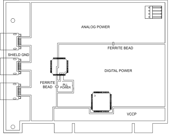
If separate power planes are used, they must be tied together at one point through a low impedance bridge or preferably through a ferrite bead (See Figure 13). Care must be taken to capacitively de-couple each power rail close to the device.
The analog ground (AGND), digital ground (DGND), and Phase Locked Loop (PLL) ground (PLLGND) must be tied together to the low impedance circuit board ground plane.
 Figure 13. A Image Plane Partition, Route Signal Carefully
11.1.3 Image Planes
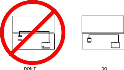
An image plane is a layer of copper (voltage plane or ground plane), physically adjacent to a signal routing plane. Use of image planes provides a low impedance, shortest possible return path for RF currents. For a 1394 board the best image plane is the ground plane, since on most designs a common ground can be used for both analog and digital circuits. Care should be taken not to route traces such that they cross from one plane to the other, as this can cause a broken RF return path resulting in an EMI radiating loop (See Figure 7). This is important for higher frequency or repetitive signals. Therefore it is best to run all clock signals on the signal plane above a solid ground plane (on a multi-layer board). Avoid crossing the image power or ground plane boundaries with high speed clock signal traces immediately above or below the separated planes. This also holds true for the twisted pair signals (TPA, TPB). Special care should be applied to the LPS and LKON signals as these do not always route easily on a single layer.
Any unused area of the top and bottom signal layers of the PCB can be filled with copper that is connected to the ground plane through vias.
 Figure 14. Do Not Cross Image Plane Boundaries
Care should also be taken not to overlap planes that do not reference each other. For example do not overlap a digital power plane with an analog power plane as this will produce a capacitance between the overlapping area which could pass RF emissions from one plane to the other. See Figure 15.
 Figure 15. Do Not Overlap Planes
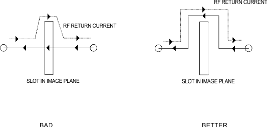
Avoid image plane violations. Traces that route over a slot in an image plane results in a possible RF return loop. See Figure 16.
 Figure 16. Do Not Violate Image Planes
11.1.4 Parts Placement
Components should be placed on the board such that the traces coming from a component will always be above its corresponding image plane. The PHY should also be placed close to the link to reduce the trace length of the PHY/link interface. For less radiated EMI, place the PHY device as far away from the 1394 connector (termination network should be close to the PHY) as is practical. Balance this against keeping the twisted pair trace lengths short (for signal integrity), keeping the PHY-Link interface traces short (for signal integrity and EMI) and keeping the PHY away from any switching power supply.
11.1.5 Decoupling Capacitors
Properly used decoupling caps keep RF energy from being injected into the power planes from high frequency components. Decoupling capacitors also provides a localized source of pulsed DC power for device or components. This reduces peak current surges from propagating across the board. Use 0.1 µF and 0.001 µF decoupling caps on the PHY and link (For PLLVDD see Power Supply Recommendations. Minimize the trace length between the decoupling capacitor and the corresponding power pins on the device. Also minimize the trace length from the capacitor pad to the power or ground plane. See Figure 17.
 Figure 17. Decoupling Capacitors
11.1.6 3W Rule for SCLK
When routing the SCLK trace from the PHY to link, try to use the 3W spacing rule. The distance from the center of the SCLK trace to the center of any adjacent signal trace should be at least three times the width of the SCLK trace. SCLK is a 49.152 MHz clock with a fast rise time. Using the 3W rule will cut down on crosstalk between traces. In general, leave space between each of the traces running from the PHY to link. Avoid using right angles when routing traces to minimize the routing distance and impedance discontinuities.
For further protection from crosstalk, run guard traces beside the SCLK signal from PHY to Link (GND pin to GND pin if possible). This is to lessen clock signal coupling onto the other PHYLink interface traces near it and thus radiating the clock signal from more antennas. See Figure 18.
 Figure 18. 3W Rule