JAJSND0
September 2024
TUSB1021-Q1
PRODUCTION DATA
1
1
特長
2
アプリケーション
3
概要
4
Pin Configuration and Functions
5
Specifications
5.1
Absolute Maximum Ratings
5.2
ESD Ratings
5.3
Recommended Operating Conditions
5.4
Thermal Information
5.5
Electrical Characteristics
5.6
Timing Requirements
5.7
Switching Characteristics
5.8
Typical Characteristics
6
Parameter Measurement Information
7
Detailed Description
7.1
Overview
7.2
Functional Block Diagram
7.3
Feature Description
7.3.1
USB 3.2
7.3.2
4-Level Inputs
7.3.3
Receiver Linear Equalization
7.4
Device Functional Modes
7.4.1
USB 3.2 2:1 MUX Description
7.4.2
Linear EQ Configuration
7.4.3
USB3.2 Modes
7.4.4
Operation Timing – Power Up
7.5
Programming
7.5.1
TUSB1021-Q1 I2C Target Behavior
8
Application and Implementation
8.1
Application Information
8.2
Typical Application
8.2.1
Design Requirements
8.2.2
Detailed Design Procedure
8.2.2.1
ESD Protection
8.2.3
Application Curve
8.3
Power Supply Recommendations
8.4
Layout
8.4.1
Layout Guidelines
8.4.2
Layout Example
9
Register Maps
9.1
General Register (address = 0x0A) [reset = 00000001]
9.2
USB3.2 Control/Status Registers (address = 0x20) [reset = 00000000]
9.3
USB3.2 Control/Status Registers (address = 0x21) [reset = 00000000]
9.4
USB3.2 Control/Status Registers (address = 0x22) [reset = 00000000]
10
Device and Documentation Support
10.1
ドキュメントの更新通知を受け取る方法
10.2
サポート・リソース
10.3
Trademarks
10.4
静電気放電に関する注意事項
10.5
用語集
11
Revision History
12
Mechanical, Packaging, and Orderable Information
パッケージ・オプション
メカニカル・データ(パッケージ|ピン)
RGF|40
MPQF173F
サーマルパッド・メカニカル・データ
発注情報
jajsnd0_oa
6
Parameter Measurement Information
Figure 6-1
I
2
C Timing Diagram Definitions
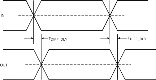
Figure 6-2
Propagation Delay
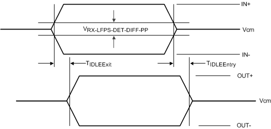
Figure 6-3
Electrical Idle Mode Exit and Entry Delay
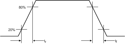
Figure 6-4
Output Rise and Fall Times