SLLSFB2 April   2020 TUSB1146

PRODUCTION DATA.  

  1. Features
  2. Applications
  3. Description
    1.     Device Images
      1.      Simplified Schematics
  4. Revision History
  5. TUSB1146 Pin Configuration and Functions
    1.     TUSB1146 Pin Functions
  6. Specifications
    1. 6.1  Absolute Maximum Ratings
    2. 6.2  ESD Ratings
    3. 6.3  Recommended Operating Conditions
    4. 6.4  Thermal Information
    5. 6.5  Power Supply Characteristics
    6. 6.6  Control I/O DC Electrical Characteristics
    7. 6.7  USB and DP Electrical Characteristics
    8. 6.8  DCI Electrical Characteristics
    9. 6.9  Timing Requirements
    10. 6.10 Switching Characteristics
    11. 6.11 Typical Characteristics
  7. Parameter Measurement Information
  8. Detailed Description
    1. 8.1 Overview
    2. 8.2 Functional Block Diagram
    3. 8.3 Feature Description
      1. 8.3.1 USB 3.1
      2. 8.3.2 DisplayPort
      3. 8.3.3 4-level Inputs
      4. 8.3.4 Receiver Linear Equalization
    4. 8.4 Device Functional Modes
      1. 8.4.1 Device Configuration in GPIO Mode
      2. 8.4.2 Device Configuration In I2C Mode
      3. 8.4.3 DisplayPort Mode
      4. 8.4.4 Linear EQ Configuration
      5. 8.4.5 VOD modes
        1. 8.4.5.1 Linearity VOD
        2. 8.4.5.2 Limited VOD
      6. 8.4.6 Transmit Equalization
      7. 8.4.7 USB3.1 Modes
      8. 8.4.8 Downstream Facing Port Adaptive Equalization
        1. 8.4.8.1 Fast Adaptive Equalization in I2C Mode
        2. 8.4.8.2 Full Adaptive Equalization
    5. 8.5 Programming
      1. 8.5.1 Transition between Modes
      2. 8.5.2 Pseudocode Examples
        1. 8.5.2.1 Fast AEQ with linear redriver mode
        2. 8.5.2.2 Fast AEQ with limited redriver mode
        3. 8.5.2.3 Full AEQ with linear redriver mode
        4. 8.5.2.4 Full AEQ with limited redriver mode
      3. 8.5.3 TUSB1146 I2C Address Options
      4. 8.5.4 TUSB1146 I2C Slave Behavior
    6. 8.6 Register Maps
      1. 8.6.1 TUSB1146 Registers
        1. 8.6.1.1  General_1 Register (Offset = 0xA) [reset = 0x1]
          1. Table 13. General_1 Register Field Descriptions
        2. 8.6.1.2  DCI_TXEQ_CTRL Register (Offset = 0xB) [reset = 0x6C]
          1. Table 14. DCI_TXEQ_CTRL Register Field Descriptions
        3. 8.6.1.3  DP01EQ_SEL Register (Offset = 0x10) [reset = 0x0]
          1. Table 15. DP01EQ_SEL Register Field Descriptions
        4. 8.6.1.4  DP23EQ_SEL Register (Offset = 0x11) [reset = 0x0]
          1. Table 16. DP23EQ_SEL Register Field Descriptions
        5. 8.6.1.5  DisplayPort_1 Register (Offset = 0x12) [reset = 0x0]
          1. Table 17. DisplayPort_1 Register Field Descriptions
        6. 8.6.1.6  DisplayPort_2 Register (Offset = 0x13) [reset = 0x0]
          1. Table 18. DisplayPort_2 Register Field Descriptions
        7. 8.6.1.7  AEQ_CONTROL1 Register (Offset = 0x1C) [reset = 0xF0]
          1. Table 19. AEQ_CONTROL1 Register Field Descriptions
        8. 8.6.1.8  AEQ_CONTROL2 Register (Offset = 0x1D) [reset = 0x20]
          1. Table 20. AEQ_CONTROL2 Register Field Descriptions
        9. 8.6.1.9  AEQ_LONG Register (Offset = 0x1E) [reset = 0x77]
          1. Table 21. AEQ_LONG Register Field Descriptions
        10. 8.6.1.10 USBC_EQ Register (Offset = 0x20) [reset = 0x0]
          1. Table 22. USBC_EQ Register Field Descriptions
        11. 8.6.1.11 SS_EQ Register (Offset = 0x21) [reset = 0x0]
          1. Table 23. SS_EQ Register Field Descriptions
        12. 8.6.1.12 USB3_MISC Register (Offset = 0x22) [reset = 0x44]
          1. Table 24. USB3_MISC Register Field Descriptions
        13. 8.6.1.13 USB_STATUS Register (Offset = 0x24) [reset = 0x41]
          1. Table 25. USB_STATUS Register Field Descriptions
        14. 8.6.1.14 VOD_CTRL Register (Offset = 0x32) [reset = 0x40]
          1. Table 26. VOD_CTRL Register Field Descriptions
        15. 8.6.1.15 AEQ_STATUS Register (Offset = 0x3B) [reset = 0x0]
          1. Table 27. AEQ_STATUS Register Field Descriptions
  9. Application and Implementation
    1. 9.1 Application Information
    2. 9.2 Typical Application
      1. 9.2.1 Design Requirements
      2. 9.2.2 Detailed Design Procedure
        1. 9.2.2.1 USB and DP Upstream Facing Port (USB Host / DP GPU to USB-C receptacle) Configuration
        2. 9.2.2.2 USB Downstream Facing Port (USB-C receptacle to USB Host) Configuration
          1. 9.2.2.2.1 Fixed Equalization
          2. 9.2.2.2.2 Fast Adaptive Equalization
          3. 9.2.2.2.3 Full Adaptive Equalization
      3. 9.2.3 Application Curve
    3. 9.3 System Examples
      1. 9.3.1 USB 3.1 Only
      2. 9.3.2 USB 3.1 and 2 Lanes of DisplayPort
      3. 9.3.3 DisplayPort Only
  10. 10Power Supply Recommendations
  11. 11Layout
    1. 11.1 Layout Guidelines
    2. 11.2 Layout Example
  12. 12Device and Documentation Support
    1. 12.1 Receiving Notification of Documentation Updates
    2. 12.2 Community Resources
    3. 12.3 Trademarks
    4. 12.4 Electrostatic Discharge Caution
    5. 12.5 Glossary
  13. 13Mechanical, Packaging, and Orderable Information

パッケージ・オプション

メカニカル・データ(パッケージ|ピン)
サーマルパッド・メカニカル・データ
発注情報

Parameter Measurement Information

TUSB1146 Timing_Diagram_Definitions_SLLSEV7.gifFigure 17. I2C Timing Diagram Definitions
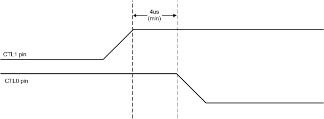
TUSB1146 USB3.1_to_4_Lane_DP_SLLSEV7.gifFigure 18. USB3.1 to 4-Lane DisplayPort in GPIO Mode
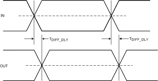
TUSB1146 Propagation_Delay_SLLSEV7.gifFigure 19. Propagation Delay
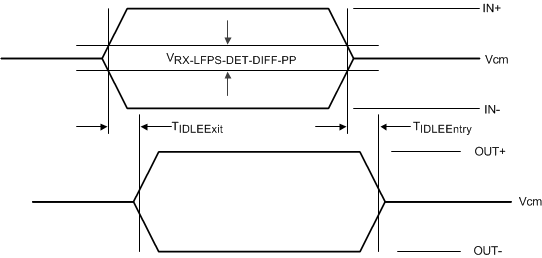
TUSB1146 Electrical_Idle_Mode_SLLSEV7.gifFigure 20. Electrical Idle Mode Exit and Entry Delay
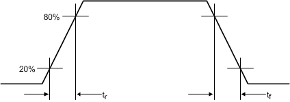
TUSB1146 Output_Rise_and_Fall_Times_SLLSEV7.gifFigure 21. Output Rise and Fall Times
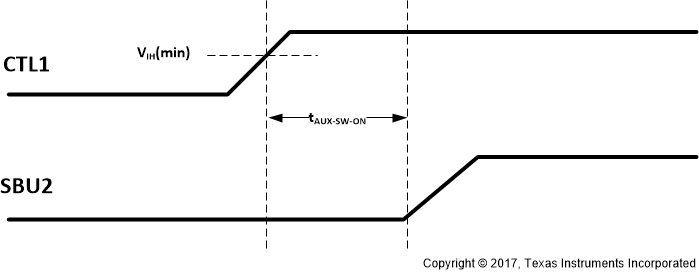
TUSB1146 AUX-SBU-ON.gifFigure 22. AUX to SBU Switch ON Timing Diagram
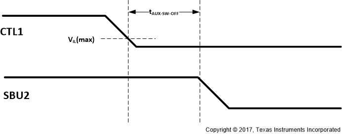
TUSB1146 AUX-SBU-OFF.gifFigure 23. AUX to SBU Switch OFF Timing Diagram
TUSB1146 TUSB546A_DCI_DCI_Clock_Propagation_Delay_SLLSF14.gifFigure 24. DCI Clock Propagation Delay
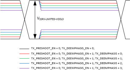
TUSB1146 TUSB1146_Deemphasis_only.gifFigure 25. SSRX Limited De-emphasis Only
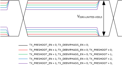
TUSB1146 TUSB1146_Preshoot_only.gifFigure 26. SSRX Limited Pre-Shoot Only
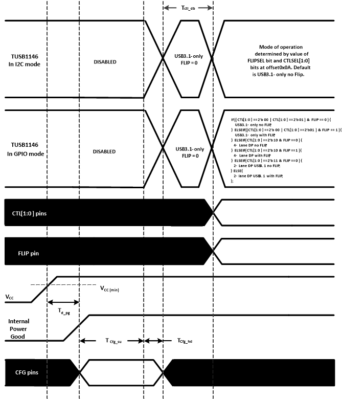
TUSB1146 TUSB1146_PWRON.gifFigure 27. Power-On Timing