SLLSE80B March 2011 – June 2015 TUSB1211
PRODUCTION DATA.
- 1Device Overview
- 2Revision History
- 3Pin Configuration and Functions
-
4Specifications
- 4.1 Absolute Maximum Ratings
- 4.2 ESD Ratings
- 4.3 Recommended Operating Conditions
- 4.4 Power Consumption Summary
- 4.5 Electrical Characteristics - Analog Output Pins
- 4.6 Electrical Characteristics - Analog Input Pins
- 4.7 Digital I/O Electrical Characteristics - Non-ULPI Pins
- 4.8 Digital I/O Electrical Characteristics - Non-ULPI Pins
- 4.9 Electrical Characteristics - REFCLK
- 4.10 Electrical Characteristics - CLOCK Input
- 4.11 Electrical Characteristics - REFCLK
- 4.12 Electrical Characteristics - CK32K Clock Generator
- 4.13 Thermal Characteristics
- 4.14 REG3V3 Internal LDO Regulator Characteristics
- 4.15 REG1V8 Internal LDO Regulator Characteristics
- 4.16 REG1V5 Internal LDO Regulator Characteristics
- 4.17 Timers and Debounce
- 4.18 OTG VBUS Electrical
- 4.19 LS/FS Single-Ended Receivers
- 4.20 LS/FS Differential Receiver
- 4.21 LS Transmitter
- 4.22 FS Transmitter
- 4.23 HS Transmitter
- 4.24 Pullup and Pulldown Resistors
- 4.25 Autoresume Watchdog Timer
- 4.26 UART Transceiver
- 4.27 OTG ID Electrical
- 4.28 Electrical Specs - Charger Detection Currents
- 4.29 Electrical Specs - Resistance
- 4.30 Electrical Specs - Capacitance
- 4.31 Charger Detection Debounce and Wait Timing
- 4.32 ULPI Interface
- 4.33 Power-On Timing Diagrams
- 4.34 Clock System
- 4.35 Clock System
- 4.36 Power Management
- 4.37 Power Provider
- 4.38 Power Control
-
5Detailed Description
- 5.1 Overview
- 5.2 Functional Block Diagram
- 5.3
Feature Description
- 5.3.1 USB On-The-Go (OTG) Feature
- 5.3.2 VBUS Detection Status Bits vs VBUS Comparators
- 5.3.3 USB Transceiver (PHY)
- 5.3.4 LS/FS Single-Ended Receivers
- 5.3.5 LS/FS Differential Receiver
- 5.3.6 LS/FS Transmitter
- 5.3.7 HS Differential Receiver
- 5.3.8 HS Differential Transmitter
- 5.3.9 Autoresume
- 5.3.10 UART Transceiver
- 5.3.11 USB On-The-Go (OTG)
- 5.3.12 USB Battery Charger Detection and ACA
- 5.3.13 USB Battery Charger Detection Modes
- 5.3.14 Accessory Charger Adapter (ACA) Detection
- 5.4
Register Maps
- 5.4.1 VENDOR_ID_LO
- 5.4.2 VENDOR_ID_HI
- 5.4.3 PRODUCT_ID_LO
- 5.4.4 PRODUCT_ID_HI
- 5.4.5 FUNC_CTRL
- 5.4.6 FUNC_CTRL_SET
- 5.4.7 FUNC_CTRL_CLR
- 5.4.8 IFC_CTRL
- 5.4.9 IFC_CTRL_SET
- 5.4.10 IFC_CTRL_CLR
- 5.4.11 OTG_CTRL
- 5.4.12 OTG_CTRL_SET
- 5.4.13 OTG_CTRL_CLR
- 5.4.14 USB_INT_EN_RISE
- 5.4.15 USB_INT_EN_RISE_SET
- 5.4.16 USB_INT_EN_RISE_CLR
- 5.4.17 USB_INT_EN_FALL
- 5.4.18 USB_INT_EN_FALL_SET
- 5.4.19 USB_INT_EN_FALL_CLR
- 5.4.20 USB_INT_STS
- 5.4.21 USB_INT_LATCH
- 5.4.22 DEBUG
- 5.4.23 SCRATCH_REG
- 5.4.24 SCRATCH_REG_SET
- 5.4.25 SCRATCH_REG_CLR
- 5.4.26 POWER_CONTROL
- 5.4.27 POWER_CONTROL_SET
- 5.4.28 POWER_CONTROL_CLR
- 5.4.29 VENDOR_SPECIFIC1
- 5.4.30 VENDOR_SPECIFIC1_SET
- 5.4.31 VENDOR_SPECIFIC1_CLR
- 5.4.32 VENDOR_SPECIFIC2_STS
- 5.4.33 VENDOR_SPECIFIC2_LATCH
- 5.4.34 VENDOR_SPECIFIC3
- 5.4.35 VENDOR_SPECIFIC3_SET
- 5.4.36 VENDOR_SPECIFIC3_CLR
- 5.4.37 VENDOR_SPECIFIC4
- 5.4.38 VENDOR_SPECIFIC4_SET
- 5.4.39 VENDOR_SPECIFIC4_CLR
- 5.4.40 VENDOR_SPECIFIC5
- 5.4.41 VENDOR_SPECIFIC5_SET
- 5.4.42 VENDOR_SPECIFIC5_CLR
- 5.4.43 VENDOR_SPECIFIC6
- 5.4.44 VENDOR_SPECIFIC6_SET
- 5.4.45 VENDOR_SPECIFIC6_CLR
- 6Application, Implementation, and Layout
- 7Device and Documentation Support
- 8Mechanical Packaging and Orderable Information
6 Application, Implementation, and Layout
NOTE
Information in the following applications sections is not part of the TI component specification, and TI does not warrant its accuracy or completeness. TI’s customers are responsible for determining suitability of components for their purposes. Customers should validate and test their design implementation to confirm system functionality.
6.1 Application Information
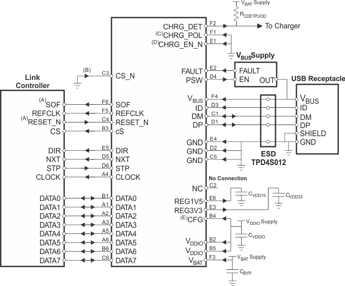
Figure 6-1 shows the suggested application diagram (host or OTG, ULPI output-clock mode).
The TUSB1211 is a USB2.0 transceiver chip, designed to interface with a USB controller through a ULPI interface. The device supports all USB2.0 data rates (high-speed, full-speed, and low-speed) and it is compliant to both host and peripheral (OTG) modes. Use Section 6.2.1 and Section 6.2.2 to select the wished operation mode. This section presents a simplified discussion of the design process.
6.2 Typical Application

6.2.1 Design Requirements
Table 6-1 Design Parameters
| DESIGN PARAMETER | EXAMPLE VALUE |
|---|---|
| VBAT | 3.3 V |
| VDDIO | 1.8 V |
| VBUS | 5 V |
| USB Support | HS, FS, LS |
| USB Battery Charger Detection | Yes |
| USB On the Go (OTG) | Yes |
| Clock sources | 26 MHz or 19.2 MHz oscillator |
6.2.2 Detailed Design Procedure
Connect the TUSB12111 device as is shown in the suggested application diagram, Figure 6-1. Follow the Board Guidelines of the Application Report, TUSB121x USB2.0 Board Guidelines (SWCA124)
Table 6-2 External Components
| FUNCTION | COMPONENT | REFERENCE | VALUE | NOTE |
|---|---|---|---|---|
| VDDIO | Capacitor | CVDDIO.IN | 100 nF | Suggested value, application dependent |
| REG3V3 | Capacitor | CREG3V3 | 2.2 µF (recommended) |
Range: [0.45 μF : 6.5 μF] ESR = [0 : 600 mΩ] for f > 10 kHz |
| REG1V5 | Capacitor | CREG1V5 | 2.2 µF (recommended) |
Range: [0.45 μF : 6.5 μF] ESR = [0 : 600 mΩ] for f > 10 kHz |
| VBAT | Capacitor | CBYP | 2.2 µF (recommended) |
Range: [0.45 μF : 6.5 μF] ESR = [0 : 600 mΩ] for f > 10 kHz |
| VBUS | Capacitor | CVBUS | 4.7 µF (recommended) | Place close to USB connector |
Table 6-3 VBUS Capacitors
| FUNCTION | COMPONENT | REFERENCE | VALUE | NOTE |
|---|---|---|---|---|
| VBUS – HOST | Capacitor | CVBUS | > 120 μF | |
| VBUS – DEVICE | Capacitor | CVBUS | 4.7 μF | Range: 1.0 μF to 10.0 μF |
| VBUS – OTG | Capacitor | CVBUS | 4.7 μF | Range: 1.0 μF to 6.5 μF |
6.2.2.1 Unused Pins Connection
- CHRG_DET Output. Leave floating if unused.
- CHRG_POL Input. Tie to GND to make CHRG_DET pin active low if unused.
- CHRG_EN_N Input. Tie to VBAT to disable dead-battery charger detection if unused.
- SOF Output. Leave floating if unused.
- REFCLK Input. If REFCLK is unused, and 60-MHz clock is provided by MODEM (60 MHz should be connected to CLOCK pin in this case) then tie REFCLK to GND.
- CFG tie to GND if REFCLK is 19.2 MHz, or tie to VDDIO if REFCLK is 26 MHz. Tie to either GND or VDDIO (do not care which) if REFCLK not used (that is, ULPI input clock configuration).
6.2.3 Application Curves


6.3 Layout
6.3.1 Layout Guidelines
- The VDDIO pins of the TUSB1211 supply 1.8 V (nominal) power to the core of the TUSB1211 device. This power rail can be isolated from all other power rails by a ferrite bead to reduce noise.
- The VBAT pin of the TUSB1211 supply 3.3 V (nominal) power rail to the TUSB1211 device. This power rail can be isolated from all other power rails by a ferrite bead to reduce noise.
- The VBUS pin of the TUSB1211 supply 5 V (nominal) power rail to the TUSB1211 device. This pin is normally connected to the VBUS pin of the USB connector.
- All power rails require 0.1-μF decoupling capacitors for stability and noise immunity. The smaller decoupling capacitors should be placed as close to the TUSB1211 device power pins as possible with an optimal grouping of two of differing values per pin.
6.3.1.1 Ground
TI recommends using almost one board ground plane be used in the design. This provides the best image plane for signal traces running above the plane. An earth or chassis ground is implemented only near the USB port connectors on a different plane for EMI and ESD purposes.
6.3.2 Layout Example
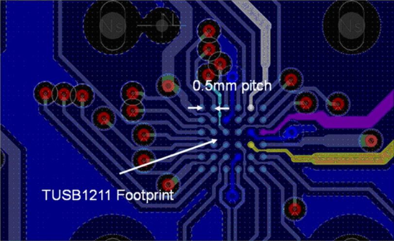
 Figure 6-4 TUSB1211 Layout
6.4 Power Supply Recommendations
VBUS, VBAT, and VDDIO are needed for power the TUSB1211 device.
The recommended operation is for VBAT to be present before VDDIO. Applying VDDIO before VBAT to the TUSB1211 device is not recommended because a diode from VDDIO to VBAT will be forward-biased when VDDIO is present but VBAT is not present. TUSB121x does not strictly require VBUS to function.