JAJSDO5A August 2017 – September 2017 TUSB212
PRODUCTION DATA.
6 Specifications
6.1 Absolute Maximum Ratings
over operating free-air temperature and voltage range (unless otherwise noted)(1)| MIN | MAX | UNIT | ||
|---|---|---|---|---|
| Supply Voltage Range | VCC | -0.3 | 3.8 | V |
| Voltage Range on I/O pins | DxP, DxM, RSTN, EQ, SCL, SDA, DC_BOOST, VREG | -0.3 | 3.8 | V |
| Tstg | Storage temperature | -65 | 150 | °C |
6.2 ESD Ratings
| VALUE | UNIT | |||
|---|---|---|---|---|
| V(ESD) | Electrostatic discharge | Human body model (HBM), per ANSI/ESDA/JEDEC JS-001, all pins(1) | ±2000 | V |
| Charged device model (CDM), per JEDEC specification JESD22-C101, all pins(2) | ±500 | |||
6.3 Recommended Operating Conditions
over operating free-air temperature and voltage range (unless otherwise noted)| MIN | NOM | MAX | UNIT | |||
|---|---|---|---|---|---|---|
| VCC | Supply Voltage | 3 | 3.3 | 3.6 | V | |
| TA | Ambient temperature | TUSB212 | 0 | 70 | °C | |
| TUSB212I | -40 | 85 | °C | |||
| TJ | Junction temperature | TUSB212 | 0 | 85 | °C | |
| TUSB212I | -40 | 105 | °C | |||
6.4 Thermal Information
| THERMAL METRIC(1) | TUSB212 | UNIT | |
|---|---|---|---|
| RWB (VQFN) | |||
| 12 PINS | |||
| RθJA | Junction-to-ambient thermal resistance | 137.4 | °C/W |
| RθJC(top) | Junction-to-case (top) thermal resistance | 62 | °C/W |
| RθJB | Junction-to-board thermal resistance | 67.2 | °C/W |
| ΨJT | Junction-to-top characterization parameter | 1.9 | °C/W |
| ΨJB | Junction-to-board characterization parameter | 67.3 | °C/W |
| RθJC(bot) | Junction-to-case (bottom) thermal resistance | N/A | °C/W |
6.5 Electrical Characteristics
over operating free-air temperature and voltage range (unless otherwise noted)| PARAMETER | TEST CONDITIONS | MIN | TYP | MAX | UNIT | |
|---|---|---|---|---|---|---|
| POWER | ||||||
| IACTIVE_HS | High-speed (HS) active curent | USB channel = HS mode; 480 Mbps traffic; VCC = 3.3V; VCC supply stable; DC Boost = 60 mV | 22 | 30 | mA | |
| IIDLE_HS | High-speed idle current | USB channel = HS mode; no traffic; VCC = 3.3V; VCC supply stable; DC Boost = 60 mV | 14 | 22 | mA | |
| ISUSPEND_HS | High-speed suspend current | USB channel = HS suspend mode; VCC = 3.3V; VCC supply stable | 0.55 | 1.5 | mA | |
| IFS_LS | Full/Low speed current | USB channel = FS mode or LS mode; VCC = 3.3V | 0.6 | 1.5 | mA | |
| IDISCONNECT | Disconnect current | Host side application; No device attachment; VCC = 3.3V | 0.7 | 1.5 | mA | |
| IRSTN | Disable current | RSTN driven low; VCC supply stable; VCC = 3.3V | 13 | 80 | µA | |
| ILKG_FS | Pin fail-safe leakage current for SDA, SCL, DC_BOOST, DxP/N, RSTN | VCC = 0 V; Pin at 3.6 V | 40 | µA | ||
| RSTN | ||||||
| VIH | High-level input voltage | VCC = 3.0V | 2 | 3.6 | V | |
| VIL | Low-level input voltage | VCC = 3.6V | 0 | 0.8 | V | |
| IIH | High-level input current | VIH = 3.6 V | -4 | 4 | µA | |
| IIL | Low-level input current | VIL = 0 V | -11 | 11 | µA | |
| EQ | ||||||
| REQ | External pull-down resistor on EQ pin. | AC Boost Level 0 | 160 | Ω | ||
| AC Boost Level 1 | 1.4 | 2 | kΩ | |||
| AC Boost Level 2 | 3.7 | 3.9 | kΩ | |||
| AC Boost Level 3 | 6 | kΩ | ||||
| CD, ENA_HS | ||||||
| VOH | High-level output voltage | IO = -50µA | 2.4 | V | ||
| VOL | Low-level output voltage | IO = 50µA | 0.4 | V | ||
| SCL, SDA | ||||||
| CI2CBUS | I2C Bus capacitance | 4 | 150 | pF | ||
| VIH | SDA and SCL input high level voltage | VCC = 3.0V | 2 | 3.6 | V | |
| VIL | SDA and SCL input low level voltage | VCC = 3.6V | 0.8 | V | ||
| VSDA_OL | SDA low level output voltage | 4.7kΩ pullup to 3.6V; VCC = 3.0V | 0.4 | V | ||
| ISDA_OL | SDA low level output current | VCC = 3.6V | 1.1 | mA | ||
| DC_BOOST | ||||||
| VIH | High-level input voltage | VCC = 3.3V | 2.4 | 3.6 | V | |
| VIM | Mid-level input voltage | VCC = 3.3V | 1.6 | V | ||
| VIL | Low-level input voltage | VCC = 3.3V | 0 | 0.4 | V | |
| DxP, DxM | ||||||
| CIO_DXX | Capacitance to GND | Measured with LCR meter and device powered down. 1 MHz sinusoid, 30 mVpp ripple | 2.4 | pF | ||
6.6 Switching Characteristics
over operating free-air temperature and voltage range (unless otherwise noted)| PARAMETER | TEST CONDITIONS | MIN | TYP | MAX | UNIT | |
|---|---|---|---|---|---|---|
| FBR_DXX | DxP/M bit rate | USB channel = HS mode; 480 Mbps traffic; VCC supply stable | 480.24 | Mbps | ||
| tRISE_DXX | DxP/M rise time | 10% - 90%; VCC = 3.6V; Max AC Gain; | 100 | ps | ||
| tFALL_DXX | DxP/M fall time | 90% - 10%; VCC = 3.6V; Max AC Gain; | 100 | ps | ||
| tRSTN_PULSE_WIDTH | Minimum width to detect a valid RSTN signal assert when the pin is actively driven | VCC = 3.0 V; Refer to Figure 1 | 20 | µs | ||
| tSTABLE | VCC stable before RSTN de-assertion | Refer to Figure 1 | 100 | µs | ||
| tVCC_RAMP | VCC ramp time | 0.2 | 100 | ms | ||
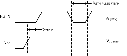 Figure 1. Power On and Reset Timing
6.7 Typical Characteristics
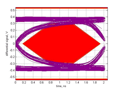 Figure 2. USB2.0 HS Eye Diagram, Host far-end with 2m cable post-channel loss without TUSB212
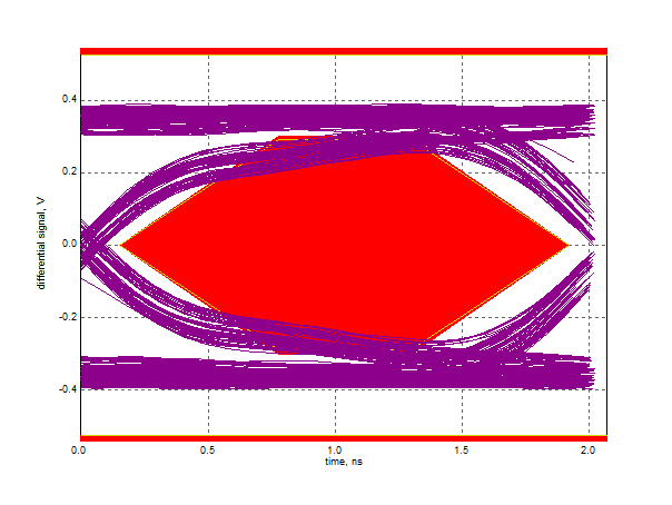 Figure 4. USB2.0 HS Eye Diagram, Host far-end with 5m cable pre-channel loss without TUSB212
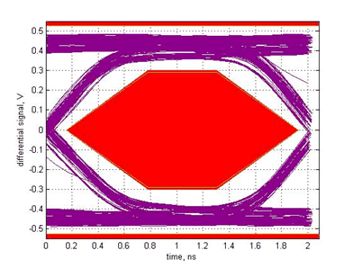 Figure 3. USB 2.0 HS Eye Diagram, Host far-end with 2m cable post-channel loss with TUSB212
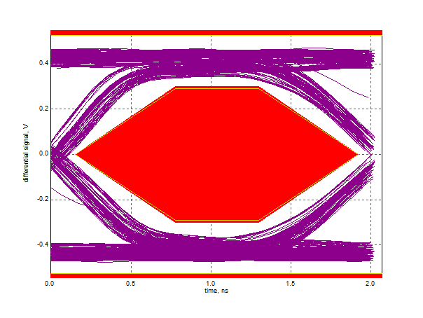 Figure 5. USB2.0 HS Eye Diagram, Host far-end with 5m cable pre-channel loss with TUSB212