JAJSDH7B June 2017 – May 2019 TUSB546A-DCI
PRODUCTION DATA.
- 1 特長
- 2 アプリケーション
- 3 概要
- 4 改訂履歴
- 5 概要(続き)
- 6 Pin Configuration and Functions
-
7 Specifications
- 7.1 Absolute Maximum Ratings
- 7.2 ESD Ratings
- 7.3 Recommended Operating Conditions
- 7.4 Thermal Information
- 7.5 Power Supply Characteristics
- 7.6 DC Electrical Characteristics
- 7.7 AC Electrical Characteristics
- 7.8 DCI Specific Electrical Characteristics
- 7.9 Timing Requirements
- 7.10 Switching Characteristics
- 7.11 Typical Characteristics
- 8 Parameter Measurement Information
-
9 Detailed Description
- 9.1 Overview
- 9.2 Functional Block Diagram
- 9.3 Feature Description
- 9.4 Device Functional Modes
- 9.5 Programming
- 9.6
Register Maps
- 9.6.1 General Register (address = 0x0A) [reset = 00000001]
- 9.6.2 DisplayPort Control/Status Registers (address = 0x10) [reset = 00000000]
- 9.6.3 DisplayPort Control/Status Registers (address = 0x11) [reset = 00000000]
- 9.6.4 DisplayPort Control/Status Registers (address = 0x12) [reset = 00000000]
- 9.6.5 DisplayPort Control/Status Registers (address = 0x13) [reset = 00000000]
- 9.6.6 USB3.1 Control/Status Registers (address = 0x20) [reset = 00000000]
- 9.6.7 USB3.1 Control/Status Registers (address = 0x21) [reset = 00000000]
- 9.6.8 USB3.1 Control/Status Registers (address = 0x22) [reset = 00000100]
- 10Application and Implementation
- 11Power Supply Recommendations
- 12Layout
- 13デバイスおよびドキュメントのサポート
- 14メカニカル、パッケージ、および注文情報
8 Parameter Measurement Information
 Figure 11. I2C Timing Diagram Definitions
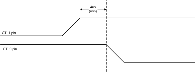
  Figure 12. USB3.1 to 4-Lane DisplayPort in GPIO Mode
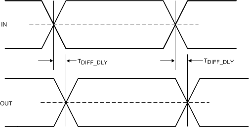
  Figure 13. Propagation Delay
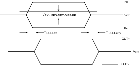
  Figure 14. Electrical Idle Mode Exit and Entry Delay
  Figure 15. Output Rise and Fall Times
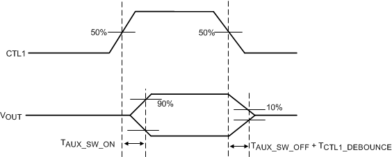
  Figure 16. AUX and SBU Switch ON and OFF Timing Diagram
  Figure 17. DCI Clock Propagation Delay