DATA SHEET
TUSB551 1.8-V USB 3.0 Single Channel Re-Driver with Equalization
1 Features
- USB3.0 SuperSpeed Re-Driver with 1.8 V Power Supply
- Ultra Low-Power Architecture:
- Active: <130 mW
- U2/U3: <22 mW
- < 8mW with No Connection
- Optimal Receiver Equalization:
- 3/6/9 dB
- Superior Drive Performance
- Automatic LFPS De-Emphasis Control To Meet USB 3.0 Certification Requirements
- No Host/Device-Side Requirement
- Small Package Options
- Hot-Plug Capable
- ESD protection exceeds > ±4kV HBM
- -40°C to 85°C Industrial Temperature Range
2 Applications
- Cell Phones
- Tablets
- Docking Stations
- Televisions
- Active Cables
- Backplanes
3 Description
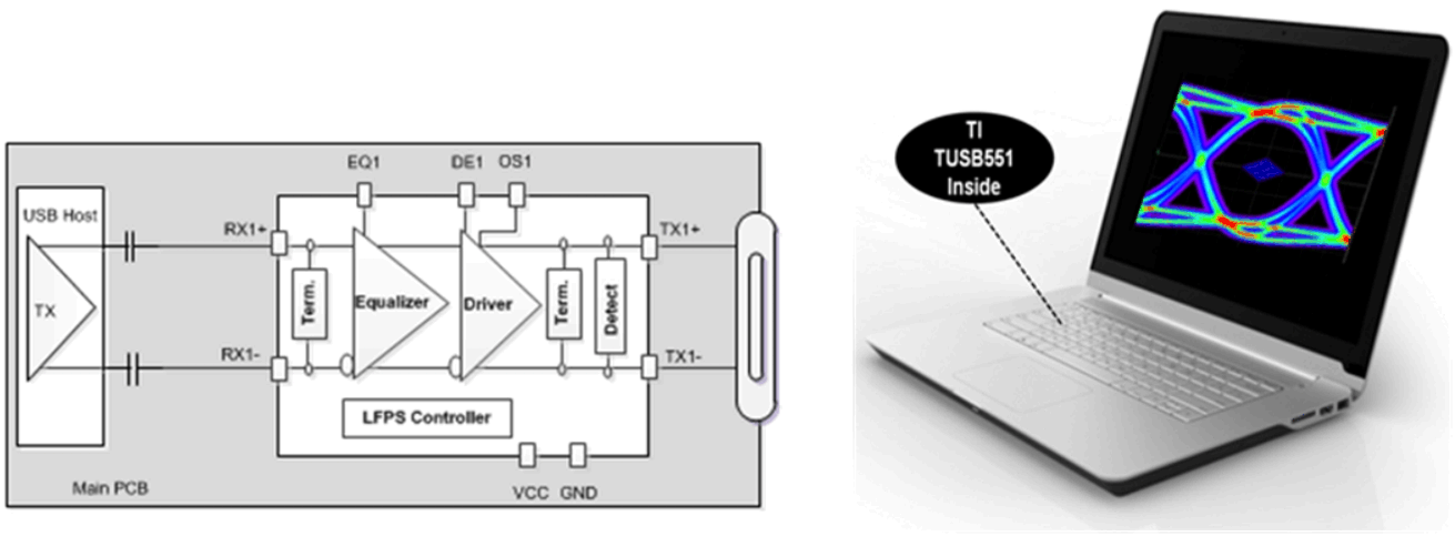
The TUSB551 is a 4th-generation USB3.0 SuperSpeed (SS) re-driver that features a 1.8V power supply with low consumption, superior output drive performance, and automatic LFPS De-Emphasis control for full USB 3.0 compliance. The re-driver offers selectable gain settings in the equalizer to account for channel loss. These settings are controlled by the EQ terminal. To compensate for downstream transmission line losses, the output driver supports configuration of De-Emphasis and Output Swing (terminals DE and OS). These settings allow optimal performance, increased signaling distance, and flexibility in placement of the TUSB551 in the SuperSpeed USB path.
Device Information
| ORDER NUMBER | PACKAGE | BODY SIZE |
|---|---|---|
| TUSB551RWBR | X2QFN (12) | 1.6mm x 1.6mm |
4 Simplified Schematic
5 Revision History
Changes from * Revision (March 2014) to A Revision
- Changed from PRODUCT PREVIEW to PRODUCTION DATA Go
6 Terminal Configuration and Functions
RWB Package
1.6 mm x 1.6 mm
(Top View)
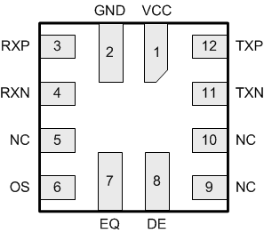
Terminal Functions
| TERMINAL | I/O | DESCRIPTION | |
|---|---|---|---|
| NAME | NO. | ||
| VCC | 1 | Power | 1.8 V Power Supply. |
| GND | 2 | GND | Ground. |
| RXP | 3 | Differential input | Differential input for 5Gbps SuperSpeed positive signals. |
| RXN | 4 | Differential input | Differential input for 5Gbps SuperSpeed negative signals. |
| NC | 5, 9, 10 | Not internally connected | |
| OS | 6 | CMOS Input | Sets output swing on the TX. 2-state input with integrated pull-up and pull-down resistors. |
| EQ | 7 | CMOS Input | Sets equalizer gain on the RX. 3-state input with integrated pull-up and pull-down resistors. |
| DE | 8 | CMOS Input | Sets output de-emphasis on the TX. 3-state input with integrated pull-up and pull-down resistors. |
| TXN | 11 | Differential output | Differential output for 5Gbps SuperSpeed negative signals. |
| TXP | 12 | Differential output | Differential output for 5Gbps SuperSpeed positive signals. |
7 Specifications
7.1 Absolute Maximum Ratings
over operating free-air temperature range (unless otherwise noted)(1)| MIN | MAX | UNIT | |||
|---|---|---|---|---|---|
| VCC | Supply voltage range | –0.3 | 2.3 | V | |
| Voltage range at any input or output terminal | Differential I/O | –0.3 | 1.5 | V | |
| CMOS Inputs | –0.3 | 2.3 | |||
| TJ | Maximum junction temperature | 105 | °C | ||
(1) Stresses beyond those listed under absolute maximum ratings may cause permanent damage to the device. These are stress ratings only and functional operation of the device at these or any conditions beyond those indicated under recommended operating conditions is not implied. Exposure to absolute-maximum-rated conditions for extended periods may affect device reliability.
7.2 Handling Ratings
| MIN | MAX | UNIT | |||
|---|---|---|---|---|---|
| TSTG | Storage temperature | –65 | 150 | °C | |
| ESD | Electrostatic discharge | Human Body Model (all terminals)(1) | ±4 | kV | |
| Charged-device model (all terminals)(2) | ±1250 | V | |||
(1) Tested in accordance with JEDEC Standard 22, Test Method A114-B.
(2) Tested in accordance with JEDEC Standard 22, Test Method C101-A.
7.3 Recommended Operating Conditions
over operating free-air temperature range (unless otherwise noted)| MIN | NOM | MAX | UNIT | ||
|---|---|---|---|---|---|
| VCC | Main power supply | 1.62 | 1.8 | 1.98 | V |
| TA | Operating free-air temperature | –40 | 85 | °C | |
| CAC | AC coupling capacitor | 75 | 100 | 200 | nF |
7.4 Thermal Information
| THERMAL METRIC(1) | TUSB551 | UNIT | |
|---|---|---|---|
| RWB PACKAGE | |||
| 12 TERMINALS | |||
| θJA | Junction-to-ambient thermal resistance(2) | 175.2 | °C/W |
| θJCtop | Junction-to-case (top) thermal resistance(3) | 71.5 | |
| θJB | Junction-to-board thermal resistance(4) | 40.5 | |
| ψJT | Junction-to-top characterization parameter(5) | 2.5 | |
| ψJB | Junction-to-board characterization parameter(6) | 40.5 | |
(1) For more information about traditional and new thermal metrics, see the IC Package Thermal Metrics application report, SPRA953.
(2) The junction-to-ambient thermal resistance under natural convection is obtained in a simulation on a JEDEC-standard, high-K board, as specified in JESD51-7, in an environment described in JESD51-2a.
(3) The junction-to-case (top) thermal resistance is obtained by simulating a cold plate test on the package top. No specific JEDEC-standard test exists, but a close description can be found in the ANSI SEMI standard G30-88.
(4) The junction-to-board thermal resistance is obtained by simulating in an environment with a ring cold plate fixture to control the PCB temperature, as described in JESD51-8.
(5) The junction-to-top characterization parameter, ψJT, estimates the junction temperature of a device in a real system and is extracted from the simulation data for obtaining θJA, using a procedure described in JESD51-2a (sections 6 and 7).
(6) The junction-to-board characterization parameter, ψJB, estimates the junction temperature of a device in a real system and is extracted from the simulation data for obtaining θJA , using a procedure described in JESD51-2a (sections 6 and 7).
7.5 Power Supply Electrical Characteristics
over operating free-air temperature range (unless otherwise noted)| PARAMETER | TEST CONDITIONS | MIN | TYP | MAX | UNIT | |
|---|---|---|---|---|---|---|
| ICC-ACTIVE | Average active current | Link in U0 with SuperSpeed data transmission; OS = Low; DE = Low | 71.65 | mA | ||
| Link in U0 with SuperSpeed data transmission; OS = Floating; DE = Low | 82.35 | |||||
| ICC-IDLE | Average current in idle state | Link has some activity, not in U1; OS = Low | 35 | mA | ||
| ICC-U2U3 | Average current in U2/U3 | Link in U2 or U3 | 12.20 | mA | ||
| ICC-NC | Average current with no connection | No SuperSpeed device is connected to TXP/TXN | 4.3 | mA | ||
7.6 DC Electrical Characteristics
over operating free-air temperature range (unless otherwise noted)| PARAMETER | TEST CONDITIONS | MIN | TYP | MAX | UNIT | |
|---|---|---|---|---|---|---|
| 3-State CMOS Inputs (EQ, DE) | ||||||
| VIH | High-level input voltage | VCC * 0.8 | V | |||
| VIM | Mid-level input voltage | VCC / 2 | V | |||
| VIL | Low-level input voltage | VCC * 0.2 | V | |||
| VF | Floating voltage | VIN = High impedance | VCC / 2 | V | ||
| RPU | Internal pull-up resistance | 105 | kΩ | |||
| RPD | Internal pull-down resistance | 105 | kΩ | |||
| IIH | High-level input current | VIN = 1.98V | 26 | µA | ||
| IIL | Low-level input current | VIN = GND | –26 | µA | ||
| 2-State CMOS Inputs (OS) | ||||||
| VIL | Low-level input voltage | VCC * 0.8 | V | |||
| VIM | Mid-level input voltage | VCC/2 | V | |||
| VF | Floating voltage | VIN = High Impedance | VCC/2 | V | ||
| RPD | Internal pull-down resistance | 105 | Ω | |||
| IIM | Mid-level input current | 26 | µA | |||
| IIL | Low-level input current | VIN = GND | -26 | µA | ||
7.7 AC Electrical Characteristics
over operating free-air temperature range (unless otherwise noted)| PARAMETER | TEST CONDITIONS | MIN | TYP | MAX | UNIT | |
|---|---|---|---|---|---|---|
| Differential Receiver (RXP, RXN) | ||||||
| VCM-RX | Common-mode voltage bias in the receiver (DC) | 0 | V | |||
| ZRX-DIFF | Differential input impedance (DC) | Present after a SuperSpeed device is detected on TXP/TXN | 72 | 91 | 120 | Ω |
| ZRX-CM | Common-mode input impedance (DC) | Present after a SuperSpeed device is detected on TXP/TXN | 18 | 24 | 30 | Ω |
| ZRX-HIGH-IMP-DC-POS | Common-mode input impedance with termination disabled (DC) | Present when no SuperSpeed device is detected on TXP/TXN. Measured over the range of 0-500mV with respect to GND. | 25 | 150 | kΩ | |
| VRX-LFPS-DET-DIFF-PP | Low Frequency Periodic Signaling (LFPS) detect threshold | Below the minimum is squelched. | 100 | 300 | mVpp | |
| CRX | RX input capacitance to GND | At 2.5GHz | 400 | fF | ||
| Differential Transmitter (TXP, TXN) | ||||||
| VTX-DIFF-PP | Transmitter differential voltage swing (transition-bit)(1) | OS = Low, DE=Low | 1050 | mVpp | ||
| OS = Floating, DE=Low | 1200 | |||||
| VTX-DIFF-PP-LFPS | LFPS differential voltage swing | OS = Low, Floating | 800 | 1200 | mVpp | |
| VTX-DE-RATIO | Transmitter de-emphasis | DE = Low, OS = Floating | 0 | dB | ||
| DE = Floating, OS = Floating | –3 | –3.5 | –4 | |||
| DE = High, OS = Floating | –6 | |||||
| CTX | TX input capacitance to GND | At 2.5GHz | 1.25 | pF | ||
| ZTX-DIFF | Differential impedance of the driver | 80 | 120 | Ω | ||
| ZTX-CM | Common-mode impedance of the driver | Measured with respect to AC ground over 0-500mV | 20 | 30 | Ω | |
| ITX-SC | TX short circuit current | TX+/- shorted to GND | 60 | mA | ||
| VCM-TX | Common-mode voltage bias in the transmitter (DC) | 0.6 | 0.8 | V | ||
| VCM-TX-AC | AC common-mode voltage swing in active mode | Within U0 and within LFPS | 100 | mVpp | ||
| VTX-IDLE-DIFF -AC-PP | Differential voltage swing during electrical idle | Tested with a high-pass filter | 0 | 10 | mVpp | |
| VTX-CM-ΔU1-U0 | Absolute delta of DC CM voltage during active and idle states | 100 | mV | |||
| VTX-IDLE-DIFF-DC | DC electrical idle differential output voltage | Voltage must be low pass filtered to remove any AC component | 0 | 10 | mV | |
| Vdetect | Voltage change to allow receiver detect | Positive voltage to sense receiver termination | 600 | mV | ||
(1) VTX-DIFF-PP is measured at the TX output with no load and no trace.
7.8 Timing Requirements/Timing Diagrams
over operating free-air temperature range (unless otherwise noted)| PARAMETER | TEST CONDITIONS | MIN | TYP | MAX | UNIT | |
|---|---|---|---|---|---|---|
| tREADY | Time from power applied until RX termination | Apply 0V to VCC, connect SuperSpeed termination to TX±, apply 1.8V to VCC, and measure when ZRX-DIFF is enabled. | 52 | ms | ||
| Differential Transmitter (TXP, TXN) | ||||||
| tr, tf | Output rise/fall times (see Figure 3) | 20%-80% of differential voltage measured 1 inch from the output terminal | 56 | ps | ||
| tRF-MM | Output rise/fall time mismatch | 20%-80% of differential voltage measured 1 inch from the output terminal | 2.6 | ps | ||
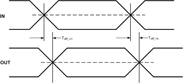 Figure 1. Propagation Delay Timing
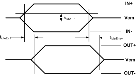 Figure 2. Electrical Idle Mode Exit and Entry Delay Timing
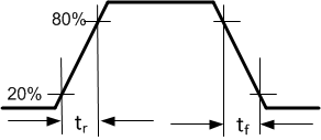 Figure 3. Output Rise and Fall Times
7.9 Switching Characteristics
over operating free-air temperature range (unless otherwise noted)| PARAMETER | TEST CONDITIONS | MIN | TYP | MAX | UNIT | |
|---|---|---|---|---|---|---|
| Differential Transmitter (TXP, TXN) | ||||||
| Tdiff-LH, Tdiff-HL | Differential propagation delay times (see Figure 1) | De-Emphasis = –3.5dB Propagation delay between 50% level at input and output | 278 | ps | ||
| tidleEntry, tidleExit | Idle entry and exit times (see Figure 2) | 6 | ns | |||
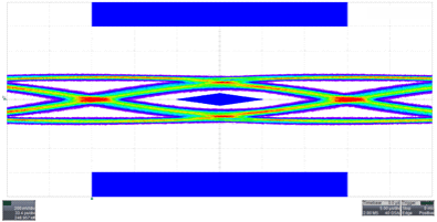
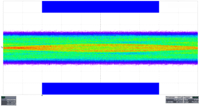
7.10 Typical Characteristics
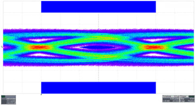
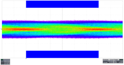
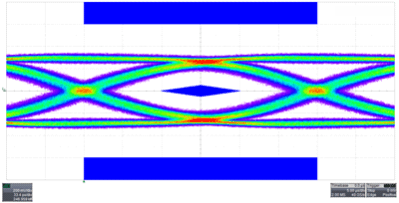
Output = 4”+3m Cable
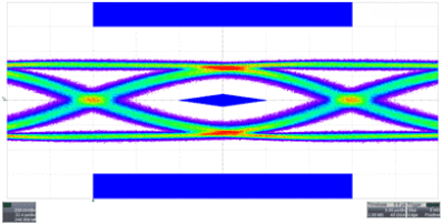
Output = 4”+3m Cable