JAJSGO2H November 2006 – August 2020 TXB0108
PRODUCTION DATA
- 1 特長
- 2 アプリケーション
- 3 概要
- 4 Revision History
- 5 Pin Configuration and Functions
-
6 Specifications
- 6.1 Absolute Maximum Ratings
- 6.2 Handling Ratings
- 6.3 Recommended Operating Conditions
- 6.4 Thermal Information
- 6.5 Electrical Characteristics
- 6.6 Timing Requirements: VCCA = 1.2 V
- 6.7 Timing Requirements: VCCA = 1.5 V ± 0.1 V
- 6.8 Timing Requirements: VCCA = 1.8 V ± 0.15 V
- 6.9 Timing Requirements: VCCA = 2.5 V ± 0.2 V
- 6.10 Timing Requirements: VCCA = 3.3 V ± 0.3 V
- 6.11 Switching Characteristics: VCCA = 1.2 V
- 6.12 Switching Characteristics: VCCA = 1.5 V ± 0.1 V
- 6.13 Switching Characteristics: VCCA = 1.8 V ± 0.15 V
- 6.14 Switching Characteristics: VCCA = 2.5 V ± 0.2 V
- 6.15 Switching Characteristics: VCCA = 3.3 V ± 0.3 V
- 6.16 Operating Characteristics
- 6.17 Typical Characteristics
- 7 Parameter Measurement Information
- 8 Detailed Description
- 9 Application and Implementation
- 10Power Supply Recommendations
- 11Layout
- 12Device and Documentation Support
- 13Mechanical, Packaging, and Orderable Information
パッケージ・オプション
デバイスごとのパッケージ図は、PDF版データシートをご参照ください。
メカニカル・データ(パッケージ|ピン)
- ZXY|20
- YZP|20
- NME|20
- DQS|20
- PW|20
- RGY|20
サーマルパッド・メカニカル・データ
発注情報
13.1.1 Tape and Reel Information
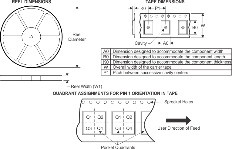
*All dimensions are nominal
| Device | Package Type | Package Drawing | Pins | SPQ | Reel Diameter (mm) | Reel Width W1 (mm) | A0 (mm) | B0 (mm) | K0 (mm) | P1 (mm) | W (mm) | Pin1 Quadrant |
|---|---|---|---|---|---|---|---|---|---|---|---|---|
| TXB0108DQSR | USON | DQS | 20 | 3000 | 177.8 | 12.4 | 2.21 | 4.22 | 0.81 | 4.0 | 12.0 | Q1 |
| TXB0108RGYR | VQFN | RGY | 20 | 3000 | 330.0 | 12.4 | 3.8 | 4.8 | 1.6 | 8.0 | 12.0 | Q1 |
| TXB0108YZPR | DSBGA | YZP | 20 | 3000 | 180.0 | 8.4 | 1.99 | 2.49 | 0.56 | 4.0 | 8.0 | Q1 |
| TXB0108YZPR2 | DSBGA | YZP | 20 | 3000 | 180.0 | 8.4 | 1.99 | 2.49 | 0.56 | 4.0 | 8.0 | Q2 |
| TXB0108ZXYR | BGA MICROSTAR JUNIOR | ZXY | 20 | 2500 | 330.0 | 12.4 | 2.8 | 4.22 | 3.3 | 1.0 | 12.0 | Q2 |
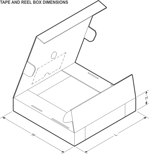
| Device | Package Type | Package Drawing | Pins | SPQ | Length (mm) | Width (mm) | Height (mm) |
|---|---|---|---|---|---|---|---|
| TXB0108DQSR | USON | DQS | 20 | 3000 | 202.0 | 201.0 | 28.0 |
| TXB0108RGYR | VQFN | RGY | 20 | 3000 | 355.0 | 350.0 | 50.0 |
| TXB0108YZPR | DSBGA | YZP | 20 | 3000 | 182.0 | 182.0 | 20.0 |
| TXB0108YZPR2 | DSBGA | YZP | 20 | 3000 | 182.0 | 182.0 | 20.0 |
| TXB0108ZXYR | BGA MICROSTAR JUNIOR | ZXY | 20 | 2500 | 336.6 | 336.6 | 28.6 |