JAJSQ37 july   2023 TXV0106-Q1

ADVANCE INFORMATION  

  1.   1
  2. 特長
  3. アプリケーション
  4. 概要
  5. Revision History
  6. Pin Configuration and Functions
  7. Specifications
    1. 6.1 Absolute Maximum Ratings
    2. 6.2 ESD Ratings
    3. 6.3 Recommended Operating Conditions
    4. 6.4 Thermal Information
    5. 6.5 Electrical Characteristics
    6. 6.6 Switching Characteristics, VCCA = 1.8 ± 0.15 V
    7. 6.7 Switching Characteristics, VCCA = 2.5 ± 0.2 V
    8. 6.8 Switching Characteristics, VCCA = 3.3 ± 0.3 V
  8. Parameter Measurement Information
    1. 7.1 Load Circuit and Voltage Waveforms
  9. Detailed Description
    1. 8.1 Overview
    2. 8.2 Functional Block Diagram
    3. 8.3 Feature Description
      1. 8.3.1 Balanced High-Drive CMOS Push-Pull Outputs
      2. 8.3.2 Partial Power Down (Ioff)
      3. 8.3.3 VCC Isolation and VCC Disconnect (Ioff-float)
      4. 8.3.4 Over-Voltage Tolerant Inputs
      5. 8.3.5 Negative Clamping Diodes
      6. 8.3.6 Fully Configurable Dual-Rail Design
      7. 8.3.7 Supports High-Speed Translation
    4. 8.4 Device Functional Modes
  10. Application and Implementation
    1. 9.1 Application Information
    2. 9.2 Typical Application
      1. 9.2.1 Design Requirements
      2. 9.2.2 Detailed Design Procedure
      3. 9.2.3 Application Curves
    3. 9.3 Power Supply Recommendations
    4. 9.4 Layout
      1. 9.4.1 Layout Guidelines
      2. 9.4.2 Layout Example
  11. 10Device and Documentation Support
    1. 10.1 Documentation Support
      1. 10.1.1 Related Documentation
    2. 10.2 ドキュメントの更新通知を受け取る方法
    3. 10.3 サポート・リソース
    4. 10.4 Trademarks
    5. 10.5 静電気放電に関する注意事項
    6. 10.6 用語集
  12. 11Mechanical, Packaging, and Orderable Information
    1. 11.1 Tape and Reel Information
    2. 11.2 Mechanical Data

パッケージ・オプション

メカニカル・データ(パッケージ|ピン)
サーマルパッド・メカニカル・データ
発注情報

Load Circuit and Voltage Waveforms

Unless otherwise noted, all input pulses are supplied by generators having the following characteristics:

  • f = 1 MHz
  • ZO = 50 Ω
  • Δt/ΔV ≤ 1 ns/V

GUID-F69EA5FA-85D4-4CF2-BD87-F449FB37C9BE-low.gif
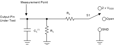
CL includes probe and jig capacitance.
Figure 7-1 Load Circuit
Table 7-1 Load Circuit Conditions
ParameterVCCORLCLS1VTP
tpdPropagation (delay) time1.65 V – 3.6 V2 kΩ

15 pF

OpenN/A
ten, tdisEnable time, disable time1.65 V – 3.6 V2 kΩ15 pF2 × VCCO0.15 V
ten, tdisEnable time, disable time1.65 V – 3.6 V2 kΩ15 pFGND0.15 V
GUID-29B55282-BD14-42BC-A482-2405CBD9DFDD-low.gif
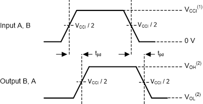
  1. VCCI is the supply pin associated with the input port.
  2. VOH and VOL are typical output voltage levels that occur with specified RL, CL, and S1
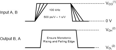
Figure 7-2 Propagation Delay
GUID-C000B029-9869-4135-B657-BD61524A75C8-low.gif
  1. VCCI is the supply pin associated with the input port.
  2. VOH and VOL are typical output voltage levels that occur with specified RL, CL, and S1
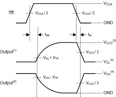
Figure 7-3 Input Transition Rise and Fall Rate
GUID-6D38ACC0-6D77-4DEA-9BC7-BD598F2068FC-low.gif
Output waveform on the condition that input is driven to a valid Logic Low.
Output waveform on the condition that input is driven to a valid Logic High.
VCCO is the supply pin associated with the output port.
VOH and VOL are typical output voltage levels with specified RL, CL, and S1.
Figure 7-4 Enable Time and Disable Time