JAJSEH2G November 1970 – January 2018
PRODUCTION DATA.
- 1 特長
- 2 アプリケーション
- 3 概要
- 4 改訂履歴
- 5 Pin Configurations and Functions
- 6 Specifications
- 7 Detailed Description
- 8 Application and Implementation
- 9 Power Supply Recommendations
- 10Layout
- 11デバイスおよびドキュメントのサポート
- 12メカニカル、パッケージ、および注文情報
パッケージ・オプション
メカニカル・データ(パッケージ|ピン)
サーマルパッド・メカニカル・データ
- PS|8
発注情報
6.8 Typical Characteristics
Data at high and low temperatures are applicable only within the rated operating free-air temperature ranges of the various devices.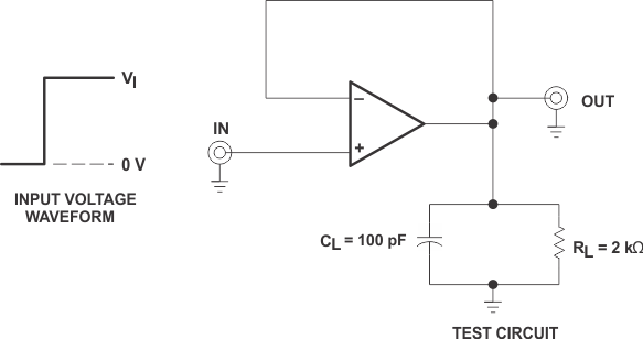 Figure 1. Rise Time, Overshoot, and Slew Rate
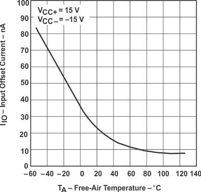 Figure 2. Input Offset Current vs Free-Air Temperature
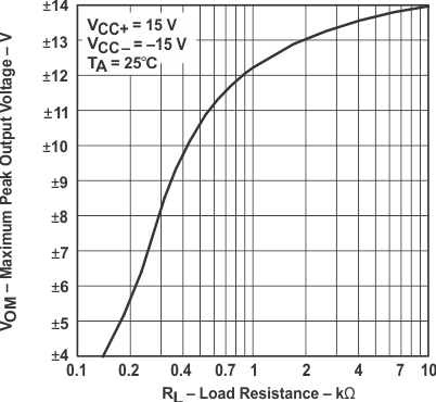 Figure 4. Maximum Output Voltage vs Load Resistance
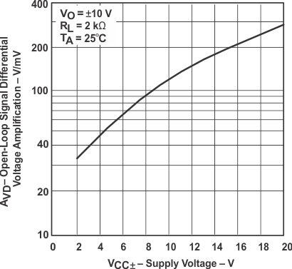 Figure 6. Open-Loop Signal Differential Voltage Amplification vs Supply Voltage
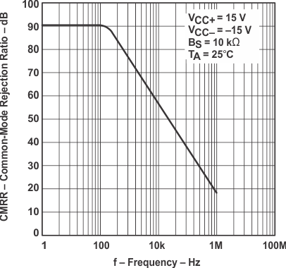 Figure 8. Common-Mode Rejection Ratio vs Frequency
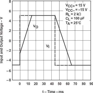 Figure 10. Voltage-Follower Large-Signal Pulse Response
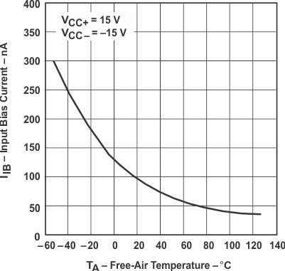 Figure 3. Input Bias Current vs Free-Air Temperature
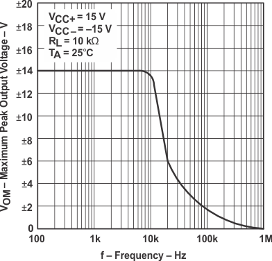 Figure 5. Maximum Peak Output Voltage vs Frequency
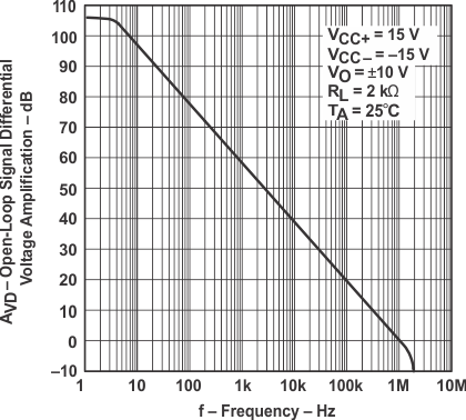 Figure 7. Open-Loop Large-Signal Differential Voltage Amplification vs Frequency
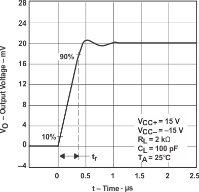 Figure 9. Output Voltage vs Elapsed Time