SLUSAG0A March 2011 – March 2016 UC1707-SP
PRODUCTION DATA.
- 1 Features
- 2 Applications
- 3 Description
- 4 Revision History
- 5 Pin Configuration and Functions
- 6 Specifications
- 7 Parameter Measurement Information
- 8 Detailed Description
- 9 Application and Implementation
- 10Power Supply Recommendations
- 11Layout
- 12Device and Documentation Support
- 13Mechanical, Packaging, and Orderable Information
パッケージ・オプション
メカニカル・データ(パッケージ|ピン)
サーマルパッド・メカニカル・データ
発注情報
8 Detailed Description
8.1 Overview
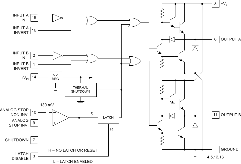
UC1707-SP was designed specifically as a power MOSFET driver for switching-mode power supply applications. It is capable of providing fast transitions and high-peak current required by power MOSFETs. One of the most important factors while developing the UC1707-SP was to isolate the high speed switching noise from the low level analog signals at the PWM. Separate supply and return paths at the driver signal inputs and power outputs further enhance noise immunity.
8.2 Functional Block Diagram

8.3 Feature Description
8.3.1 Shutdown Circuit Description
The function of the circuitry is to be able to provide a shutdown of the device. This is defined as functionality that will drive both outputs to the low state. There are three different inputs that govern this shutdown capability.
- Analog Stop Pins — The differential inputs to this comparator provide a way to execute a shutdown.
- Latch Disable Pin — Assuming that the Shutdown pin is left open, a high on this pin disables the latching functionality of the Analog Stop shutdown. A low on this pin enables the latching functionality of the Analog Stop shutdown. If a shutdown occurs through the Analog Stop circuit while Latch Disable is high, then the outputs will go low, but will return to normal operation as soon as the Analog Stop circuit allows it. If a shutdown occurs through the Analog Stop circuit while Latch Disable is low, then the outputs will go low and remain low even if the Analog Stop circuit no longer drives the shutdown. The outputs will remain "latched" low (in shutdown) until the Latch Disable goes high and the Analog Stop circuit allows it to return from shutdown or the VIN voltage is cycled to 0 V and then returned above 5 V.
- Shutdown Pin — This pin serves two purposes.
- It can be used as an output of the Analog Stop circuit.
- It can be used as an input to force a shutdown or to force the device out of shutdown. This pin can override both the Analog Stop circuit as well as the Latch Disable Pin. When driving hard logic levels into the Shutdown pin, the Latch Disable functionality will be overridden and the Latch Disable will not function as it does when used in conjunction with the Analog Stop circuit. When the Shutdown pin is high, the outputs will be in the low state (shutdown). When the Shutdown pin is low (hard logic low) the outputs will operate normally, regardless of the state of the Latch Disable pin or the Analog Stop pins.
To use the Shutdown Pin with the Latch Disable functional it is necessary to use either a diode in series with the Shutdown signal or to use an open collector pullup so that the Shutdown pin is not pulled low. This configuration will allow the Latch Disable function to work with the Shutdown pin.
8.4 Device Functional Modes
Table 1. UG1707 Shutdown Truth Table
| ANALOG STOP LOGIC | SHUTDOWN | LATCH DISABLE | PREVIOUS STATE OF OUTPUT | OUTPUT |
|---|---|---|---|---|
| X | 0 | X | X | Follows Input Logic |
| X | 1 | X | X | Low (Shutdown) |
| 1 | Open | X | X | Low (Shutdown) |
| 0 | Open | 0 | Shutdown | Latched Shutdown(1) |
| 0 | Open | 0 | Normal | Follows Input Logic |
| 0 | Open | 1 | X | Follows Input Logic |