SLUSAG0A March 2011 – March 2016 UC1707-SP
PRODUCTION DATA.
- 1 Features
- 2 Applications
- 3 Description
- 4 Revision History
- 5 Pin Configuration and Functions
- 6 Specifications
- 7 Parameter Measurement Information
- 8 Detailed Description
- 9 Application and Implementation
- 10Power Supply Recommendations
- 11Layout
- 12Device and Documentation Support
- 13Mechanical, Packaging, and Orderable Information
パッケージ・オプション
メカニカル・データ(パッケージ|ピン)
サーマルパッド・メカニカル・データ
発注情報
5 Pin Configuration and Functions
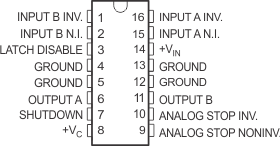
J or W Package
16-Pin CDIP or CFP
Top View

All four ground pins must be connected to a common ground.
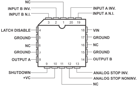
FK Package
20-Pin LCCC
Top View

Pin Functions
| PIN | I/O | DESCRIPTION | |||
|---|---|---|---|---|---|
| NAME | CDIP | LCCC | CFP | ||
| INPUT B INVERTING | 1 | 2 | 1 | I | Inverting TTL compatible input threshold. |
| INPUT B NONINVERTING | 2 | 3 | 2 | I | Non-Inverting TTL compatible input threshold. |
| LATCH DISABLE | 3 | 4 | 3 | I | Assuming SHUTDOWN pin is left open, a high on this pin disables the latching functionality of the analog stop shutdown. |
| GROUND | 4 | 5 | 4 | - | |
| GROUND | 5 | 7 | 5 | - | |
| OUTPUT A | 6 | 8 | 6 | O | Output is a 1.5 A totem-pole driver optimized for MOSFET gates. |
| SHUTDOWN | 7 | 9 | 7 | I | Used as an output of the analog stop circuit. Also used as an input to force shutdown or to force the device out of shutdown. |
| +VC | 8 | 10 | 8 | I | Collector supply voltage. |
| ANALOG STOP (+) | 9 | 12 | 9 | I | This pin is normally connected to a reference voltage used for comparison with the sensed power supply output voltage level at the E/A (+) pin. |
| ANALOG STOP (–) | 10 | 13 | 10 | I | This pin is normally connected to the voltage divider resistors which sense the power supply output level. |
| OUTPUT B | 11 | 14 | 11 | O | Output is a 1.5 A totem-pole driver optimized for MOSFET gates. |
| GROUND | 12 | 15 | 12 | - | All voltages are measured with respect to ground (GND). |
| GROUND | 13 | 17 | 13 | - | All voltages are measured with respect to ground (GND). |
| +VIN | 14 | 18 | 14 | I | Supply voltage. |
| INPUT A NONINVERTING | 15 | 20 | 15 | I | Non-Inverting TTL compatible input threshold. |
| INPUT A INVERTING | 16 | 19 | 16 | I | Inverting TTL compatible input threshold. |
| NC | 16 | ||||
| NC | 11 | ||||
| NC | 6 | ||||
| NC | 1 | ||||